Strain and Temperature Dependence of Defect Formation at AlGaN/GaN - PowerPoint PPT Presentation
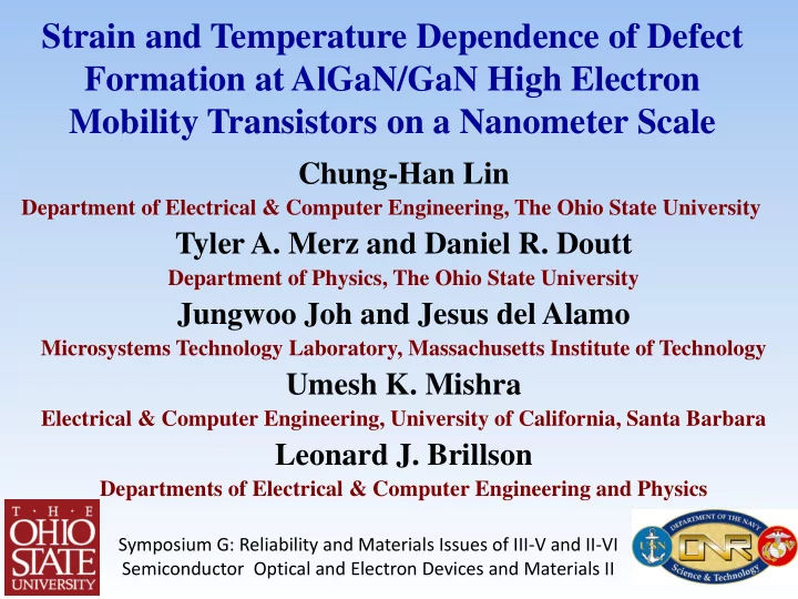
Strain and Temperature Dependence of Defect Formation at AlGaN/GaN High Electron Mobility Transistors on a Nanometer Scale Chung-Han Lin Department of Electrical & Computer Engineering, The Ohio State University Tyler A. Merz and Daniel R.
Strain and Temperature Dependence of Defect Formation at AlGaN/GaN High Electron Mobility Transistors on a Nanometer Scale Chung-Han Lin Department of Electrical & Computer Engineering, The Ohio State University Tyler A. Merz and Daniel R. Doutt Department of Physics, The Ohio State University Jungwoo Joh and Jesus del Alamo Microsystems Technology Laboratory, Massachusetts Institute of Technology Umesh K. Mishra Electrical & Computer Engineering, University of California, Santa Barbara Leonard J. Brillson Departments of Electrical & Computer Engineering and Physics Symposium G: Reliability and Materials Issues of III-V and II-VI Semiconductor Optical and Electron Devices and Materials II
Outline Background : AlGaN/GaN HEMT physical degradation mechanisms – Historical efforts Techniques: DRCLS, KPFM, I D &I GOFF vs. V DS Device Conditions: ON-state vs. OFF-state stress Electric field vs. Thermal stress : Surface potential, leakage current, defect generation Failure prediction Conclusions: (1) Dominant impact of V DS vs. I DS on device reliability (2) Primary defects located inside AlGaN
Motivation AlGaN/GaN HEMT: high power, RF, and high speed applications Reliability challenge: Hard to predict failure High current, piezoelectric material, & high field due to high bias Defect generation Micro-CL, AFM, and KPFM: Follow evolution of potential, defects, and failure
Background: All-Optical Methods [1] M. Kuball et al. IEEE Electron Device Lett. Shigekawa et al. J. Appl. Phys. 92 , 531 (2002) 23 , 7 (2002) PL Technique [2] A. Sarau et al. IEEE Trans. Electron Devices, 53 , 2438 (2006) Raman/IR Technique
Background: Scanned Probe Methods T versus Gate-Drain Location Lin et al . Appl. Phys. E G versus T Lett., 95 , 033510 (2009) A. P. Young et al., Appl. Phys. Lett, 77 , 699 (2000) Aubry et al. IEEE Transactions on Electron Device, 54 , 385 (2007) SThM Technique DRCLS Technique
Depth and Laterally-Resolved CLS T, σ , defects, atomic composition Gate source Drain AlGaN 2DEG GaN Buffer layer JEOL JAMP 7800F : SEM, Micro-CL Substrate Grading AlGaN AlN AlGaN 0.0035 GaN 5 kV, 10 nm beam 0.0030 1 keV 0.0025 2 keV Intentisty (a.u.) (25%) 3 keV 0.0020 4 keV 5 keV 0.0015 (10%) 0.0010 50 nm 0.0005 10 nm 0.0000 0 20 40 60 80 100 120 140 160 180 200 Depth (nm)
Background: Temperature Maps W.D. Hu et al . J. Appl. Phys. 100 , 074501 (2006) I. Ahmad et al. Appl. Phys. Lett. 86 , 173503 (2005) • Hottest spot at drain-side gate edge • Hot spots also inside GaN buffer September 19-24 2010 Tampa, Florida, USA C.-H. Lin et al , IEEE Trans. Electron Devices
Electroluminescence Results: Gap States Nakao et al. Jpn. J. Appl. Phys., 41 , 1990 (2002) Meneghesso et al. IEEE Tran. Device Mater. Rel., 8 , 332 (2008) 80 ° C 10 ° C Electroluminescence detects gap states forming inside Bouya et al . Microelectron. Reliab., 48 , 1366 (2008) HEMT during operation
Electrochemically-Produced Defects Park et al. Microelectron. Reliab., 49 , 478 (2009) High C, O, and Si concentrations at gate foot “lattice disruption” area Gate leakage current promotes Smith et al . ECS Transactions, 19 , 113 (2009) electrochemical reaction
Impact of Structural Defects Chowdhury et al. IEEE Electron Device Lett. 29 , 1098 (2008) Park et al . Microelectron. Reliab. 49 , 478 (2009) High field at drain - side gate can form structural defects that affect I G-OFF & I D Joh et al. IEEE Electron Dev. September 19-24 2010 Tampa, Florida, USA Lett. 29 , 287 (2008)
Inverse Piezoelectric Effect and Defects Joh et al. Microelectron. Reliab., 50 , 767 (2010) Very high local strain fields del Alamo et al . Microelectron. Reliab., 49 , 1200 (2009) piezo → strain energy V DS + V inv Sarua et al . Appl, Phys. Lett., 88 , → exceed elastic energy of crystal 103502 (2006) → form defects at gate foot
Measurement Strategy • Thermal Mapping : DRCLS NBE laterally (<10 nm) & in depth (nm’s to µm’s) – Obtain T vs. I DS ; locate “hot” spots • Stress Mapping : DRCLS NBE near gate foot vs. V DS with I DS OFF ( no heating ) • Potential Mapping : Kelvin work function vs. V DS with I DS OFF ( no heating ) • Device testing : Step-wise ON & OFF-state I DMAX and I GOFF vs. V DS • Defect Generation : CLS defect peak intensities vs. thermal and electrical stress • Defect Localization: DRCLS intensities vs. depth
Stress Conditions Reference: No stress ON-state stress : high I D , low V DS Gate Upper (I D = 0.75 A/mm, V DS = 6 V, V G = 0 V) Source Drain OFF-state stress : low I D , high V DS Lower (I D = 5*10 -6 A/mm, V DS = 10 ~ 30 V V G = -6 V) AFM & KPFM I GOFF taken at V DS = 0.5 V, V GS = -6 V scanning area Aim: Test electric field-induced strain vs. current- induced (e.g., heating) mechanism
Strain Measurements: Drain-side Gate Foot Band Gap vs. V DG Strain vs. V DG ON-state Applied voltage blue-shifts band gap, increases mechanical strain at drain-side gate foot 26 meV CL shift = 1 GPa ; V DG = 32 V 0.27 GPa C.H. Lin et al. Appl. Phys. Lett. 97 , 223502 (2010)
I DMAX , I G-OFF vs. Time & Applied Voltage ON-state OFF-state OFF-state I G-Off rises sharply at threshold V DG ON-state I G-OFF decreases vs. time → device degradation with external stress
Surface Potential Evolution (OFF-state) G D S C.H. Lin et al. Appl. Phys. Low potential regions appear and expand Lett. 97 , 223502 (2010) with increasing applied stress V DG
Surface Potential Evolution (ON-state) G D S Current stress seems to degrade device in a different way
Device Failure under OFF-state Stress Before failure After failure Gate Gate Source Source Failure area Drain Drain • Device failure occurs as V DG increases further • Large, cratered failure area appears; morphology of drain metal exhibits huge change
Correlation between AFM, KFPM & SEM AFM SEM KPFM Source 15 μ m Gate Drain After failure Before failure AFM, KPFM and SEM results reveal that device fails at the lowest surface potential area, where defect density is highest
Defect Spectroscopy of Low Potential Region Within low potential region and at depth of 2DEG, DRCLS reveals formation of deep level defects C.H. Lin et al. Appl. Phys. Lett. 97 , 223502 (2010)
Defect Generation vs. Location Areas of highest defect intensities Lower defect creation and highest stress correlate for On-state stress Largest defect increase at lowest potential region C.-H. Lin et al , IEEE Trans. Electron Devices
Defect Generation vs. Potential Increasing defects densities correlate with decreasing potential
Surface Potential vs. Electrical Stress C.H. Lin et al. Appl. Phys. Lett. 97 , 223502 (2010) 12 /cm 2 ) 1 10 Defect density (10 Normalized Averaged Surface Potential OFF-state Δ V 1.5 1.0 σ - = σ 0 /[1+exp[(E F – E a )/kT]] Φ 0.5 q Δ V = q 2 σ a d/ ε 0.0 E C 8 nm -0.5 E F 7 nm -1.0 9 nm E T -1.5 A3 -2.0 A4 A5 E V -2.5 A6 -3.0 0 5 10 15 20 25 30 35 40 • E F moves lower in gap as V DG (Volt) Normalized Averaged Surface Potential acceptor-like defects increase A1 1.0 • Drain-side surface potential A2 0.8 decreases ( Φ increases) with 0.6 increasing V DG 0.4 • Above V DG threshold, faster 0.2 decreases at low Φ patches 0.0 -0.2 • Higher Φ patches 0 5 10 15 20 25 30 35 40 decrease slower V DG (Volt)
CLS Energy Comparison with Trap Spectroscopy • DLOS: 3 traps observed: E C -0.55 (dominant), 1.1, &1.7-1.9 eV High DLOS 10 12 cm -2 Trap Density : A. R. Arehart, A. C. Malonis, C. Poblenz, Y. Pei, J. S. Speck, U. K Mishra, S. A. Ringel, Phys. Stat. Sol. C 1-3 (2011) DOI 10.1002/pssc.201000955 • DRCLS: 2.8 eV BB and 2.3 eV YB emissions: Traps that grow under DC stress – high 10 12 cm -2 densities E C 0.55 eV 1.35 eV E C 0.55 eV 1.1 eV 3.6 eV AlGaN 2.8 eV GaN 2.8 eV 4.1~4.2 eV 2.3 eV 3.4 eV E V E V KPFM E a = 0.55 Activation Energy : S. Kamiya, M. Iwami, T. Tsuchiya, M. Kurouchi, J. Kikawa, T. Yamada, A. Wakejima, H. Miyamoto, A. Suzuki, A. Hinoki, T. Araki, and Y. Nanishi, Appl. Phys. Lett. 90 , 213511 (2007); M. Arakawa, S. Kishimoto, and T. Mizutani, Jpn. J. Appl. Phys. Part I 36 , 1826 (1997)
AlGaN/GaN HEMT Defect Location Pre-stress Post-stress Source Source Before stress After stress – source side After stress – drain side 2.2 Drain Drain • New 3.6 eV feature 0.5-0.6 eV below E C → BB defect within AlGaN • Larger 2.2 eV threshold feature → higher YB defects with stress • Higher Drain-side vs. Source-side changes: consistent with DRCLS
AlGaN/GaN HEMT Physical Degradation Mechanisms Strain- and Field-induced Impurity Diffusion Inverse Piezoelectric Effect M. Kuball, et al., Microelectron. Reliab . 51 , 195 (2011) del Alamo et al . Microelectron. Electronically-Active Reliab., 49 , 1200 (2009) Defect Formation Multiple possible mechanisms that all create electronically- active defects
Recommend
More recommend
Explore More Topics
Stay informed with curated content and fresh updates.
