Status of High Gradient Tests of Single Cell Standing Wave - PowerPoint PPT Presentation
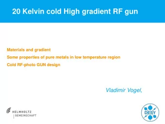
Status of High Gradient Tests of Single Cell Standing Wave Structures at SLAC Valery Dolgashev, SLAC National Accelerator Laboratory International Workshop on Linear Colliders 2010 , October 18 - 21th, 2010, Geneva, Switzerland CERN, CICG
Status of High Gradient Tests of Single Cell Standing Wave Structures at SLAC Valery Dolgashev, SLAC National Accelerator Laboratory International Workshop on Linear Colliders 2010 , October 18 - 21th, 2010, Geneva, Switzerland CERN, CICG
Outline • Motivation • Planned experiments • Recent results – Geometry – Hard materials
This work is made possible by the efforts of SLAC’s – S. Tantawi (US High Gradient Collaboration spokesperson), A. Yeremian (day-to-day operation and coordination of TS4, etc .), J. Lewandowski (rf measurements, software and TS6-TS8 operation, etc. ) of Accelerator Technology Research – E. Jongewaard, C. Pearson, A. Vlieks, J. Eichner, D. Martin, C. Yoneda, L. Laurent, A. Haase, R. Talley, J. Zelinski, J. Van Pelt, R. Kirby and staff of Klystron Lab. – Z. Li , Advanced Computation In close collaboration with: – Y. Higashi, KEK, Tsukuba, Japan – B. Spataro, INFN, Frascati, Italy
Single Cell Accelerator Structures Goals • Study rf breakdown in practical accelerating structures: dependence on circuit parameters, materials, cell shapes and surface processing techniques Difficulties • Full scale structures are long, complex, and expensive Solution • Single cell standing wave (SW) structures with properties close to that of full scale structures • Reusable couplers We want to predict breakdown behavior for practical structures
Reusable coupler: TM 01 Mode Launcher Pearson’s RF flange Cutaway view of the mode launcher Two mode launchers Surface electric fields in the mode launcher E max = 49 MV/m for 100 MW S. Tantawi, C. Nantista
Yasuo Higashi, KEK
3C-SW-A5.65-T4.6-Cu-KEK#2 installed in the lead box, 15 November 2007
High Power Tests of Single Cell Standing Wave Structures Tested • Low shunt impedance, a/lambda = 0.215, 1C-SW-A5.65-T4.6-Cu , 5 tested • Low shunt impedance, TiN coated, 1C-SW-A5.65-T4.6-Cu-TiN , 1 tested • Three high gradient cells, low shunt impedance, 3C-SW-A5.65-T4.6-Cu, 2 tested • High shunt impedance, elliptical iris, a/lambda = 0.143, 1C-SW-A3.75-T2.6-Cu , 1 tested • High shunt impedance, round iris, a/lambda = 0.143, 1C-SW-A3.75-T1.66-Cu , 1 tested • Low shunt impedance, choke with 1mm gap, 1C-SW-A5.65-T4.6-Choke-Cu , 2 tested • Low shunt impedance, made of CuZr, 1C-SW-A5.65-T4.6-CuZr, 1 tested • Low shunt impedance, made of CuCr, 1C-SW-A5.65-T4.6-CuCr, 1 tested • Highest shunt impedance copper structure 1C-SW-A2.75-T2.0-Cu , 1 tested • Photonic-Band Gap, low shunt impedance, 1C-SW-A5.65-T4.6-PBG-Cu, 1 tested • Low shunt impedance, made of hard copper 1C-SW-A5.65-T4.6-Clamped, 1 tested • Low shunt impedance, made of molybdenum 1C-SW-A5.65-T4.6-Mo, 1 tested • Low shunt impedance, hard copper electroformed 1C-SW-A5.65-T4.6-Electroformed-Cu, 1 tested • High shunt impedance, choke with 4mm gap, 1C-SW-A3.75-T2.6-4mm-Ch-Cu, 2 tested • High shunt impedance, elliptical iris, a/lambda = 0.143, 1C-SW-A3.75-T2.6-6NCu , 1 tested • High shunt impedance, elliptical iris, a/lambda = 0.143, 1C-SW-A3.75-T2.6-6N-HIP-Cu , 1 tested • High shunt impedance, elliptical iris, a/lambda = 0.143, 1C-SW-A3.75-T2.6-7N-Cu , 1 tested • Low shunt impedance, made of CuAg, 1C-SW-A5.65-T4.6-CuAg-SLAC-#1, 1 tested • High shunt impedance hard CuAg structure 1C-SW-A3.75-T2.6-LowTempBrazed-CuAg, 1 tested • High shunt impedance soft CuAg, 1C-SW-A3.75-T2.6-CuAg , 1 tested • High shunt impedance hard CuZr, 1C-SW-A3.75-T2.6-Clamped-CuZr , 1 tested • High shunt impedance dual feed side coupled, 1C-SW-A3.75-T2.6-2WR90-Cu, 1 tested • High shunt impedance single feed side coupled ,1C-SW-A3.75-T2.6-1WR90-Cu-SLAC-#1, 1 tested • High shunt impedance hard CuCr, 1C-SW-A3.75-T2.6-Clamped-CuCr , 1 tested Now 32 nd test is about to start, single feed side coupled 3C-SW-A3.75-T2.6-2WR90-Cu-SLAC-#2
Next experiments, as for October 2010 New diagnostics: High shunt impedance, full choke cell with a viewport, 1C-SW-A3.75-T2.6-Ch-View-Port-Cu Geometry tests: Photonic-Band Gap, low shunt impedance, elliptical rods, 1C-SW-A5.65-T4.6-PBG2-Cu High shunt impedance, triple choke, copper, 1C-SW-A3.75-T2.6-4mm-TripleCh-Cu High shunt impedance, reduced magnetic field, copper 1C-SW-A3.75-T2.2-Cu (see Jeff Neilson’s talk) Materials: High shunt impedance, made of hard CuAg, 1C-SW-A3.75-T2.6-Clamped-CuAg, Highest shunt impedance, made of hard CuCr, CuAg, CuZr, 1C-SW-A2.75-T2.0-Clamped-CuCr, CuAg, CuZr High shunt impedance, triple choke, Molybdenum, 1C-SW-A3.75-T2.6-4mm-TripleCh-Mo High shunt impedance, Cu-Mo, 1C-SW-A3.75-T2.6-Cu-Mo High shunt impedance, Cu-Stainless Steel, 1C-SW-A3.75-T2.6-Cu-SUS Highest shunt impedance, cryogenic test, 1C-SW-A2.75-T2.0-Cryo-Cu High shunt impedance, Stainless Steel coated with copper, 1C-SW-A3.75-T2.6-SUS-Coated-Cu Reproducibility tests: High shunt impedance, round iris, 1C-SW-A3.75-T1.66-Cu Three high gradient cells, low shunt impedance, 3C-SW-A5.65-T4.6-Cu
New diagnostics In-situ microscopic observation of surface change and rf breakdowns: Full cell choke and two view ports 1C-SW-A3.75-T2.6-Ch-View-Port-Cu-SLAC-#1,2 Solid model: David Martin, 28 April 2010
Geometry and material test Structure joining techniques that avoid high temperature treatment 1C-SW-A3.75-T2.2-Cu,Mo-KEK, 1C-SW-A3.75-T2.6-Clamped-CuAg-KEK similar configuration is under development in INFN-Frascati Y. Higashi, KEK
Material test 1C-SW-A3.75-T2.6-Clamped-CuAg-KEK Y. Higashi, KEK
Material test 1C-SW-A3.75-T2.60-Cu-SUS-Clamped-KEK Ag coated SUS gaskets Y. Higashi, KEK
Material test 1C-SW-A3.75-T2.60-Cu-Mo-Clamped-KEK Y. Higashi, KEK
Material test, electropolishing After Before electropolishing Y. Higashi, KEK
Material testing, Mo spattering on Cu SEM Picture of copper dish machined at very low roughness sputtered with Schematic diagram of a DC magnetron 300nm of Molybdenum after a thermal plasma source treatment of 2 hours at 300 C. B. Spataro, INFN-Frascati
Results • Geometry test 1C-SW-A3.75-T2.6-1WR90-Cu-SLAC-#1 • Material test 1C-SW-A3.75-T2.6-Clamped-CuCr-SLAC-#1
Geometry test High shunt-impedance single-feed side- coupled 1C-SW-A3.75-T4.6-1WR90-Cu-SLAC-#1
Side-coupled ingle feed 1C-SW-A3.75-T2.6-1WR90-Cu-SLAC-#1 Calculating Zenghai’s geometry with HFSS, driven, 10 MW input 800 Maximum magnetic field 800 kA/m, H 1WR90 / H SLANS = 412 1.198 Maximum electric field 412 MV/m, E 1WR90 / E SLANS = 1.033 668 (SLANS 1C-SW-T3.75-A2.6-Cu 668.0 kA/m) 398.9 (SLANS 398.9 MV/m ) 1 0.5 M 1 Im Im M n1 1 0 Im M n2 1 0.5 1 1 0.5 0 0.5 1 Re M 1 Re M n1 1 Re M n2 1 Resonant frequency 11.4197 GHz 10 3 f Qo 2 4.309 floor n1 n2 3854 Maximum on axis peak electric field 385 MV/m, field balance 1.012 2 10 3 4.309 10 3 1872 1936 f n1 f n2 Qo 8.618 (SLANS 384 MV/m) V.A. Dolgashev, 7 June 2010
Single-feed side-coupled structure 1C-SW-A3.75-T2.6-1WR90-Cu-SLAC-#1, Dependence of breakdown rate for different pulse length of flat part of the shaped pulse. Breakdown Probability [1/pulse/meter] Breakdown Probability [1/pulse/meter] 10 0 10 0 400 ns 600 ns 10 -1 10 -1 600 ns 10 -2 10 -2 400 ns 200 ns 10 -3 10 -3 200 ns 10 -4 10 -4 10 -5 10 -5 10 -6 10 -6 10 -7 10 -7 20 40 60 80 100 120 140 80 100 120 140 160 180 200 Peak Pulse Heating [deg . C] Gradient [MV/m]
Comparison of side-coupled copper structure with on- axis coupled copper structures of same iris geometry (1C-SW-A3.75-T2.6-Cu), shaped pulse with 150 ns flat part Breakdown Probability [1/pulse/meter] Breakdown Probability [1/pulse/meter] 10 0 10 0 10 -1 on-axis 10 -1 side-coupled 10 -2 coupled 10 -2 on-axis 10 -3 10 -3 coupled 10 -4 side-coupled 10 -4 10 -5 10 -5 a 0.143, t 2.6mm, 1WR90 Cu 10 -6 a 0.143, t 2.6mm, 1WR90 Cu a 0.143, t 2.6mm, Cu 10 -6 a 0.143, t 2.6mm, Cu 10 -7 10 -7 80 100 120 140 160 180 200 20 40 60 80 100 120 140 Gradient [MV/m] Peak Pulse Heating [deg . C] No obvious increase of breakdown rate due to increased pulse heating on coupler edges.
Comparison of one side-coupled copper structure with three on-axis coupled copper structures of same iris geometry (1C-SW-A3.75-T2.6-Cu), shaped pulse with 150 ns flat part Breakdown Probability [1/pulse/meter] Breakdown Probability [1/pulse/meter] 10 0 10 0 on-axis side-coupled 10 -1 10 -1 coupled 10 -2 10 -2 on-axis 10 -3 10 -3 coupled side-coupled 10 -4 10 -4 10 -5 10 -5 a 0.143, t 2.6mm, 1WR90 Cu a 0.143, t 2.6mm, 1WR90 Cu a 0.143, t 2.6mm, Cu a 0.143, t 2.6mm, Cu 10 -6 a 0.143, t 2.6mm, 7NCu 10 -6 a 0.143, t 2.6mm, 7NCu a 0.143, t 2.6mm, 6N HIP Cu a 0.143, t 2.6mm, 6N HIP Cu 10 -7 10 -7 80 100 120 140 160 180 200 20 40 60 80 100 120 140 Gradient [MV/m] Peak Pulse Heating [deg . C]
1C-SW-A3.75-T4.6-1WR90-Cu-SLAC-#1
Coupling cell of 1C-SW-A3.75-T4.6-1WR90-Cu-SLAC-#1
Coupling cell of 1C-SW-A3.75-T4.6-1WR90-Cu-SLAC-#1
|E×H*|@10MW rf loss Surface loss Im|E×H*| Fields are normalized to 10MW of total rf loss. Coupling cell of 1C-SW-A3.75-T4.6-1WR90-Cu-SLAC-#1
|E×H*|@10MW rf loss Surface loss Im|E×H*| Fields are normalized to 10MW of total rf loss. Coupling cell of 1C-SW-A3.75-T4.6-1WR90-Cu-SLAC-#1
|E×H*|@10MW rf loss Surface loss Surface electric fields Im|E×H*| Fields are normalized to 10MW of total rf loss. Coupling cell of 1C-SW-A3.75-T4.6-1WR90-Cu-SLAC-#1
Material test High shunt-impedance, hard-CuCr, 1C-SW-A3.75-T2.6-Clamped-CuCr- SLAC-#1
Clamped structure assembly Mechanical design: David Martin
Recommend
More recommend
Explore More Topics
Stay informed with curated content and fresh updates.
