Shock Compensation Who are we? Team members: Max Madore Joseph - PowerPoint PPT Presentation
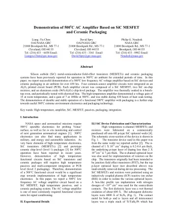
VCSO Mechanical Shock Compensation Who are we? Team members: Max Madore Joseph Hiltz-Maher Shaun Hew Shalin Shah Advisor: Helena Silva Phonon contact: Scott Kraft Project Overview VCSO and mechanical vibration Analog filter for
VCSO Mechanical Shock Compensation
Who are we? Team members: Max Madore Joseph Hiltz-Maher Shaun Hew Shalin Shah Advisor: Helena Silva Phonon contact: Scott Kraft
Project Overview • VCSO and mechanical vibration • Analog filter for compensation of 20dB • Expand compensation to three axes
Original Goals • Measure Instantaneous Frequency shifts and compare with accelerometer voltage output • Design Compensation circuit based on frequency/voltage characteristics • Test in and implement in 3 axis to determine the unique responses of each
Previous Work Last Year: • Creation of Shock Tower for repeatable tests • Comparison of two identical VCSOs • Measurement Using Oscilloscope Problems: • Unreliable Data • Mismatched VCSO frequencies
Frequency Matching VCSO Frequency Generator • Nominal frequency of • Allows for precise matching 400MHz to VCSO • Embedded Quartz crystal • Controllable down to 10Hz with varactor • Voltage controlled with linear sensitivity between roughly 1V and 3V
Phase Frequency Detector • 2 inputs (Generator and VCSO) • Output fed to operational amplifier for hardware filtering of noise and amplification for display Matched frequencies result in DC voltage
Shock Tower • Product of previous work, controlled by 24 V source with intensity controlled by duration of pulse (typically 1.5ms) • Foam Coating provides mechanical damping to reduce aftershock effects such as ringing • Connected to DAQ which allows MATLAB program to shock during data collection period
Accelerometer • ADXL001-500Z • Mounted to VCSO directly, responds synchronously with VCSO to feedback attenuated voltage. • Output of Accelerometer was measured at 2.43V, changes with sensitivity of +3.3mV/G • Fall semester we looked at raw data • Spring semester involved filtering and attenuation for compensation
Data Acquisition Card
Test Setup Shock Accelerometer Filter VCSO Signal Phase Frequency Generator Detector Filter DAQ PC
Frequency Response VSCO • The Control pin bias voltage ranges from 0-5 volts. • Linearity of the frequency response was seen between 0-2 volts. • Changes in frequency in linear region was 1.6kHz under standard operating region of 1.0-1.1V .
Problem solved with PFD • Maximum Output of the VSCO is approximately 10-12 dbm. • Maximum input of phase frequency detector is 13 dbm. • Attenuator was inserted in line with VSCO to reduce input voltage and eliminate noise. • Improve data acquisition and protect the integrity of the component.
Shocking VCSO by tapping • 3 finger tapping on VCSO appears to knock output signal out of phase • Response remains at that phase until the other shock before it goes even further out of phase. • Total phase shift represent the sum of the three individual shocks
Shocking by Solenoid • Shocking by solenoid did not produce consistent data as finger tapping after repeat trials • Results were inconsistent because more vibrations occur in SAW and possibly electromagnetic effect.
Problem with Accelerometer • Accelerometer output was too high which exceeds input voltage on VSCO of 5V. • Output of accelerometer produced oversensitive signals
Pre-Spring Break Results Filtering: • Software lowpass butterworth filter
Pre-Spring Break Results Tap Testing: • EM interference • Code revised for manual tapping • Insignificant disturbances
Pre-Spring Break Results Differential Op-Amp • Low-noise • DAQ inputs changed to single-ended • Hardware + software filtering • Wider voltage range • O-scope test point
Post Spring Break
Vibration Reduction • Oscillators secured with nylon straps • VCSO’s shimmed internally • Wires taped and organized
New Accelerometers • Faulty accelerometer: • ADXL001-500 • Only accelerometer in possession before spring break • Output magnitude 5x too large • Saturation at accelerations < 100g • Confirmed with calibrated accelerometer • New accelerometers: • Also ADXL001-500 • Single axis • 500g • 22kHz bandwidth • Able to measure the acceleration levels necessary
Acceleration Sensitivity • New accelerometers to move forward • Most important task to achieving compensation • Data processing and noise filtering have paid off • Test each axis and superimpose compensations • Accelerometer Output Attenuation Equation: • Γ = Acceleration Sensitivity (1/g) • F o = Oscillator Frequency (Hz) • m = Frequency Control Curve Slope (Hz/V) • S = Accelerometer Sensitivity (V/g)
Compensation Circuit • Potentiometers for fine tuning attenuation level • Accommodates 3 axes • Operates around 1V (most linear region on the VCSO control input) • Switches to toggle compensation • Overall gain determined by VCSO acceleration sensitivity Voltage Divider VCSO Accelerometer Non-inverting Summing Amplifier
Compensation Circuit
Ghosting • Inherent with all scanning data acquisition units • Capacitor voltage does not have time to change to the proper level • Causing data corruption • Attempted Remedies • Decrease sample rate • Increase Input Switching Time • Still an issue as will be shown
Ghosting Compensation On, Sample Rate = 200kHz
Ghosting Compensation On, Sample Rate = 500kHz
X-Axis Testing X Z Y
X-Axis Testing Compensation Off
X-Axis Testing Compensation On • Actual attenuation ratio not corresponding to calculations yet • Investigate possible ghosting in x-axis compensated result
X-Axis Testing
Y-Axis Testing X Z Y
Y-Axis Testing Ghosting Effect
Y-Axis Testing Accelerometer Input Grounded (Ghosting Removed) • No compensation necessary
Y-Axis Testing
Timeline
Budget Given Materials: • National Instruments X series USB-6353 Data Acquisition Card • NI-DAQmx software • MATLAB 2009 • Giga-tronics 6060B Signal Generator • Phonon 400MHz VCSOs • B&K 9130 triple output power supply • Phase Frequency Detectors • 2x Shock Tower • Passive Circuit Components Materials to Purchase: • Accelerometers $250 • TLC2262CP op-amps $5 • Nylon Straps $25 • Phase Frequency Detectors $150 Total Cost: $430
Recommend
More recommend
Explore More Topics
Stay informed with curated content and fresh updates.
