Recent progress in large tunnel magnetoresistance junctions T. - PowerPoint PPT Presentation
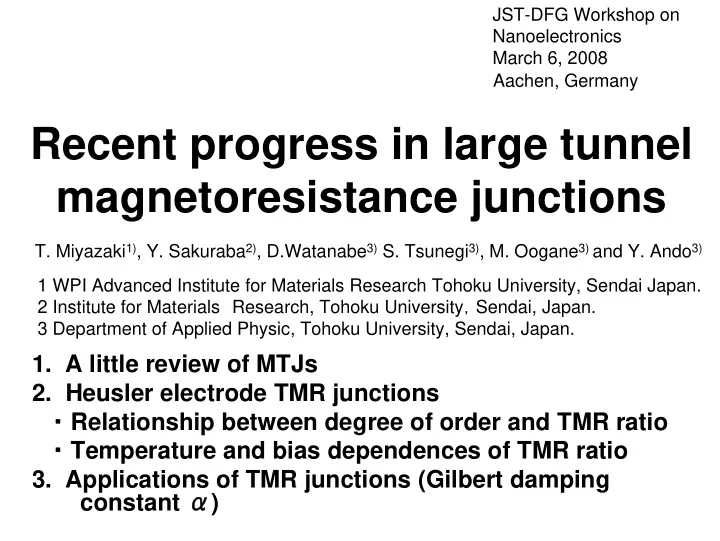
JST-DFG Workshop on Nanoelectronics March 6, 2008 Aachen, Germany Recent progress in large tunnel magnetoresistance junctions T. Miyazaki 1) , Y. Sakuraba 2) , D.Watanabe 3) S. Tsunegi 3) , M. Oogane 3) and Y. Ando 3) 1 WPI Advanced Institute
JST-DFG Workshop on Nanoelectronics March 6, 2008 Aachen, Germany Recent progress in large tunnel magnetoresistance junctions T. Miyazaki 1) , Y. Sakuraba 2) , D.Watanabe 3) S. Tsunegi 3) , M. Oogane 3) and Y. Ando 3) 1 WPI Advanced Institute for Materials Research Tohoku University, Sendai Japan. 2 Institute for Materials Research, Tohoku University , Sendai, Japan. 3 Department of Applied Physic, Tohoku University, Sendai, Japan. 1. A little review of MTJs 2. Heusler electrode TMR junctions ・ Relationship between degree of order and TMR ratio ・ Temperature and bias dependences of TMR ratio 3. Applications of TMR junctions (Gilbert damping constant α )
1. A little review of MTJs
History of TMR research (Typical reports) • Julliere (Phys. Lett., 54A ,225(1975)) Gd-O • T.Miyazaki et al. (J.Magn.Magn.Mater.139, L231 (1995)) Al-O • J.S.Moodera et al. (Phys.Rev.Lett., 74 , 3273(1995)) Al-O • • S.Yuasa et al. (Jpn.J.Appl.Phys., 43 , L588(2004)) MgO S.S.P.Parkin et al. (Nature Materials, 3 , 863(2004)) • MgO • Y.Sakuraba et al. (Appl.Phys.Lett., 88 , 192508(2006)) Heusler • • N.Tezuka et al. (Appl.Phys. Lett., 89 , 252508-1(2006)) Heusler T.Ishikawa et al. (Appl.Phys.Lett., 89 ,192505-1(2006)) Heusler •
0.008 Fe/Al 2 O 3 /Fe (a) at R. T. 20 Δ R / R S (%) R ( Ω ) 0.007 10 0 R S Magnetoresistance curve (a) and magnetic 0.006 -100 -50 0 50 100 hysteresis loop (b) for H (Oe) Fe/Al 2 O 3 /Fe junction M (arb.units) (b) T.Miyazaki and N.Tezuka, J.3M, 139 ,L2341(1995). -100 -50 50 100 H (Oe)
Fe(001)/MgO(001)/Fe(001) 300 20 K MR = 245 % 200 MR 比 ( % ) 293 K MR = 180 % 100 0 -200 -100 0 100 200 H ( Oe ) Yuasa et al. Nature Materials 3 (2004).
200 AIST Highest TMR ratio (%) (at RT) 180 160 MgO barrier 140 120 100 AIST 80 Al-O barrier NVE Sony ANELVA 60 CNRS Tohoku Fujitsu IBM 40 INESC Fujitsu Tohoku CSIC 20 IBM MIT MPI 0 1994 1995 1996 1997 1998 1999 2000 2001 2002 2003 2004 Year
600 , MgO-barrier MTJs AlO-barrier MTJs 500%@RT 500 (1010%@5K) IT- -program program IT (Ikeda et al. TMR ratio (%) of RR2002 of RR2002 400 Tohoku Univ.) AIST AIST 300 CanonANELVA & AIST CanonANELVA & AIST AIST AIST IBM 200 AIST AIST Tohoku Univ. Tohoku Univ. 100 0 1994 1996 1998 2000 2002 2004 2006 2008 Year
2. TMR in Heusler alloy electrode junction
Annalen der Physik Band 19 (1934) 155-201.
Functions of Heusler Compounds • Magnetic material: Cu 2 MnAl 1905 • Halfmetallic ferromagnet: NiMnSb 1983 • Magneto-optical: PtMnSb • Magneto-mechanic: Ni 2 MnGa • Superconductor: Pd 2 YSn From Semiconductor: CoTiSb Prof. Felser • Heavy fermion: Fe 2 VAl • Li-conductor: LiMnSb • Magneto-electronic: Co 2 FeSi 2001 • Thermo-electric: TiNiSn • Magneto-caloric: CoMnSb:Nb ・ Spintronics Material : Co 2 MnSi
X
7
UHV magnetron sputtering system (P < 1 x 10 -7 Pa) Tunneling barrier
Crystallized
We successfully fabricated highly ordered Co 2 MnSi
Giant TMR ratio over 1000% at LT is possible in CMS/(Mg/Al/Mg)-O/CMS structure 93%@RT
CoFeB/MgO/CoFeB Ikeda et al. JJAP 44 (2005) L1442 Large temperature dependence of TMR ratio should be solved.
To be published in Phys. Rev. Lett.
LSDA : Local Spin Density Appro. DMFT : Dynamical Mean Field Theory
3. Applications of TMR junction
Application of large TMR junctions • MRA (Magnetization switching : bit and word lines ) • Spin-RAM (Switching by spin transfer torque) • Magnetic reading head of HDD • GPS sensor devices • High frequency oscillator devices • • •
Magnetization switching by direct current Spin-transfer switching (STS) Slonzcewski, JMMM 159 (1996)L1 Ferro1 Spacer Ferro2 トルク STS + TMR G bit + low power MRAM New devices electron flow precession R Anti-parallel field current Current Parallel Target
Issues for Spin-RAM Gbit Mbit 10 Current field switching Spin transfer switching Writing current (mA) J = 5 × 10 6 A/ cm 2 1 × 10 6 A/ cm 2 1 Current CMOS maximum I DS 0.1 1 mA/1 μ m 5 × 10 5 A/ cm 2 CMOS Aspect ratio = 2 0.01 10 100 1000 Memory cell size (nm) Switching current : J C0 ~ 5 × 10 5 A/cm 2
Issues for device application Requirement for devices Junction Resis. 20 k Ω Area 80 × 160 nm 2 J C 0 ~ 5 × 10 5 A/cm 2 R ・ A ~ 200 Ωμ m 2 Switching current density J. C. Slonzcewski, JMMM159 (1996)L1 , PRB71(2005)024411 αγ eM d [ ] ± S J = H ± ( H + 2 π M ) / 2 c 0 ext eff S μ θ g ( P , ) B 1 P θ = g tunnel ( P , ) 2 2 ( 1 + P cos θ ) Thermal stability R. H. Koch, PRL92(2004)088302-1 τ p ⎧ − ⎫ k T Pulse width B = J J 1 ln ⎨ ⎬ c c 0 K V τ τ 0 ~ 1 ns ⎩ ⎭ u 0 α : damping constant, M s : saturation magnetization d : free layer thickness, P : spin polarization of pinned layer
Measurement of damping constant α FMR Pump-probe method Microwave bridge P u P m X-band (9.7 GHz) r p o b e H pulse h Photo-switch H i c a t s t H Kerr effect TE102 model cavity M y/ M s H 0 2 4 6 Time (ns) Line width : Δ H PP
≡ αγ ∝ − ≈ 2 G M ; G ( g 2) ; g-2 L/S S ( x 10 8 ) Fe-Co 6 Ni Wakitani et al. Fe-Ni Co-Ni CoFeB Oogane Co 2 Mn(Al,Si) G (sec -1 ) 4 Co 2 Co 2 Fe(Mn)Si (L2 1 ) ⊗ Co 2 MnAl (B2) YIG Fe 0 0 0.01 0.02 0.03 0.04 Co 2 MnSi (B2) (g-2) 2 α =0.004
Summary • TMR ratio more than 100 % (200 %) at room temperature has been obtained for Heusler electrode and Al-O (MgO) barrier tunnel junctions. • Damping constant α of Heusler alloys (Co 2 MnSi) is 0.004. • Rapid decrease of TMR ratio with raising temperature and increasing voltage can be explained by Non-quasiparticle states. • Heusler alloys are excellent candidate for spintronics materials.
ACKNOWLEDGMENTS A part of this work was supported by the IT Program of the Research Revolution 2002 (RR2002) by a Grant-in-Aid for Scientific Research from Ministry of Education, Culture, Sports, Science and Technology of Japan and by Strategic Information and Communications R&D Promotion Programme (SCOPE) by Ministry of Internal Affairs and Communications and NEDO Spintronics nonvolatile devices project.
Recommend
More recommend
Explore More Topics
Stay informed with curated content and fresh updates.

