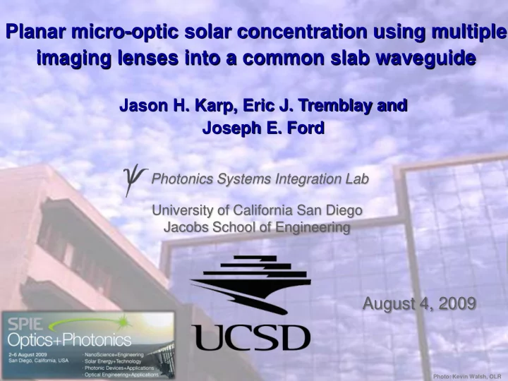
Planar micro-optic solar concentration using multiple UCSD Photonics - PowerPoint PPT Presentation
Planar micro-optic solar concentration using multiple UCSD Photonics imaging lenses into a common slab waveguide Jason H. Karp, Eric J. Tremblay and Joseph E. Ford Photonics Systems Integration Lab University of California San Diego Jacobs
Planar micro-optic solar concentration using multiple UCSD Photonics imaging lenses into a common slab waveguide Jason H. Karp, Eric J. Tremblay and Joseph E. Ford Photonics Systems Integration Lab University of California San Diego Jacobs School of Engineering August 4, 2009 Photo: Kevin Walsh, OLR PHOTONIC SYSTEMS INTEGRATION LABORATORY – UCSD JACOBS SCHOOL OF ENGINEERING 8/5/2009
Concentrator Photovoltaics (CPV) UCSD Photonics Solar Systems 1. Primary Focusing Optic SolFocus – Performs light concentration – Large collecting lens or mirror – Trend towards multiple apertures Energy Innovations 2. Secondary Homogenization Optic – Mounted between primary and PV cell – Uniform illumination for high efficiency – Non-imaging optical design Light Prescriptions Innovators Xiaohui Ning, Appl. Opt. 26 , 1987 3. Mechanical Tracking – Alignment for direct insolation – Angular acceptance defines tracking accuracy – Wind loading and environmental stability Concentrix Solar Flatcon System Tracking
Continuous Roll-to-Roll Fabrication UCSD Photonics • Continuous roll-to-roll processing – Rigid or flexible substrates – Emboss, coat and bond layers • Inexpensive mass-fabrication • Constraints: Uniform thickness Limited complexity Roll-to-Roll for CPV? Global Solar Konarka Goal: Design a uniform thickness, high-flux solar concentrator compatible with continuous roll-to-roll manufacture PHOTONIC SYSTEMS INTEGRATION LABORATORY – UCSD JACOBS SCHOOL OF ENGINEERING 8/5/2009
Micro-optic Slab Concentrator UCSD Photonics Direct Incidence Sunlight Lens Array Slab Waveguide Coupling facets Concentrated Output Advantages: – Sub-apertures couple light to single output – Homogeneous output intensity – Uniform thickness (roll-to-roll fabrication) PHOTONIC SYSTEMS INTEGRATION LABORATORY – UCSD JACOBS SCHOOL OF ENGINEERING 8/5/2009
Waveguide Coupling Facets UCSD Photonics • Reflective facets tilt light to satisfy TIR • Couplers are localized at each lens focus (<1% surface area) Waveguide Decoupling TIR Focused rays (Primary Loss) from lens Guided Rays Slab waveguide TIR TIR Reflective facet Other coupling points 120º Symmetric Prism: Repeatable structure No blocking Symmetric coupling PHOTONIC SYSTEMS INTEGRATION LABORATORY – UCSD JACOBS SCHOOL OF ENGINEERING 8/5/2009
System Layout UCSD Photonics Lens Array Waveguide Slab Waveguide Cladding Slab Thickness Geometric Concentration Ratio Slab Length C geo Slab Thickness
Coupling Facet Alignment UCSD Photonics Rotational Lateral Alignment Alignment • Align lens focus to each coupling facet • Large area concentrators (~1 meter) • >100,000 points of alignment • <50 μ m lateral alignment accuracy • <0.01° (0.2mrad) rotational alignment – Difficult over large area VERY CRITICAL Solution: Self-Alignment UV Exposure • Mold prism structure within photopolymer • Crosslink using UV exposure • Cures only at each lens focus Guarantees alignment Crosslinked regions remain part of the final concentrator PHOTONIC SYSTEMS INTEGRATION LABORATORY – UCSD JACOBS SCHOOL OF ENGINEERING 8/5/2009
Roll Processing Flowchart UCSD Photonics Lens Array UV-Curable Acrylic Superstrate Embossing Polymer and Waveguide (cont.) Emboss from Self-Alignment UV Development Coupler Master Exposure Removes Uncured Polymer PHOTONIC SYSTEMS INTEGRATION LABORATORY – UCSD JACOBS SCHOOL OF ENGINEERING 8/5/2009
Design Tradeoffs UCSD Photonics Field Displacement: Sun subtends ±0.25° θ θ f·tan θ f·tan θ d d f f Short focal length → small coupling area Long focal length → easier TIR condition Slab Length Waveguide Thickness: C flux = x Efficiency Slab Thickness Slab Slab Thickness Thickness Length Length Thick waveguide → increased efficiency Thin waveguide → high concentration PHOTONIC SYSTEMS INTEGRATION LABORATORY – UCSD JACOBS SCHOOL OF ENGINEERING 8/5/2009
Optical Model UCSD Photonics Spectrolab triple-junction cell – 240x flux concentration – 40.7% efficiency Provide 240x flux per edge System Simulation: – Model overall efficiency – Optimize design tradeoffs – Cladding options Richard R. King et al., “Advances in High -Efficiency III-V Multijunction Solar Cells,” Advances in OptoElectronics, vol. 2007 (2007). PHOTONIC SYSTEMS INTEGRATION LABORATORY – UCSD JACOBS SCHOOL OF ENGINEERING 8/5/2009
Analytic Model UCSD Photonics Simple mathematical simulation Very promising, – Scattering loss but incomplete… – Material absorption – Mirror reflectivity PHOTONIC SYSTEMS INTEGRATION LABORATORY – UCSD JACOBS SCHOOL OF ENGINEERING 8/5/2009
Zemax Raytracing Model UCSD Photonics Zemax Non-Sequential Model – Lens aberrations – Polychromatic illumination – Material dispersion – Coatings and surface reflections Includes single layer MgF 2 AR coating (@545nm) on lens array surface PHOTONIC SYSTEMS INTEGRATION LABORATORY – UCSD JACOBS SCHOOL OF ENGINEERING 8/5/2009
Broad Spectrum Performance UCSD Photonics Optimized using 0.425-1.3µm illumination – Accurate range of material models – Minimum bandwidth for multi-junction PV cells Includes single layer MgF 2 AR coating (@545nm) on lens array surface PHOTONIC SYSTEMS INTEGRATION LABORATORY – UCSD JACOBS SCHOOL OF ENGINEERING 8/5/2009
Proof-of-Concept Fabrication UCSD Photonics Goal: Demonstrate self-aligned coupling facet fabrication • Use off-the shelf components • Lens Array: Fresnel Technologies – F/1.1 hexagonal lens array 203 mm – 200 μ m image of ±0.25° source – UVT acrylic 255 mm • Waveguide: Fisher Scientific – Microscope slide (75mm x 50mm) – BK7 float glass 10 μ m field • Molding Polymer: MicroChem displacement – SU-8 Photoresist – Chemical and thermal resistances • Prism Mold: Wavefront Technology – 120° symmetric prisms – 50 μ m period, 14.4 μ m deep PHOTONIC SYSTEMS INTEGRATION LABORATORY – UCSD JACOBS SCHOOL OF ENGINEERING 8/5/2009
Fabrication Process UCSD Photonics 5. UV Exposure UV Exposure Source 1. Spin SU-8 and Softbake collimating mirror aspheric beam expansion collector and iris T 2. Apply Mold and Pull Vacuum Hg arc T 6” diameter 6. Deposit Reflective Coating beam 3. Bake Under Weight 1kg 7. Heat Above T g 4. Separate Mold and Develop and Invert Hg arc lamp Uniform, collimated UV illumination Adjust beam divergence using the iris Waveguide Un-crosslinked SU-8 Prism Mold Crosslinked SU-8 Lens Array PHOTONIC SYSTEMS INTEGRATION LABORATORY – UCSD JACOBS SCHOOL OF ENGINEERING 8/5/2009
Fabricated Couplers UCSD Photonics Al-coated prism facet 75mm Transparent glass slab 50 μ m 50mm 200 μ m 20µm Depth
Prototype Alignment UCSD Photonics Alignment stage • White light illumination – Calibrated to ±0.25° Calibrated detector • Efficiency measurement – Newport 818-ST wand detector Illuminated prototype ±0.25° Illumination • 6-axis alignment – Tolerance analysis Lens Array SUCCESSFUL COUPLING Waveguide PHOTONIC SYSTEMS INTEGRATION LABORATORY – UCSD JACOBS SCHOOL OF ENGINEERING 8/5/2009
Prototype Performance UCSD Photonics • Zemax model of prototype concentrator – Include actual lens performance and coupler size • Prototype uses off-the-shelf (non-ideal) components Prototype lens characteristics 37.5x : Fabricated Concentration Ratio PHOTONIC SYSTEMS INTEGRATION LABORATORY – UCSD JACOBS SCHOOL OF ENGINEERING 8/5/2009
Prototype Loss Mechanisms UCSD Photonics Lens array Coupler annulus • Lens F-Number – 72.5% fill factor – Spherical aberration – Coupler annulus (50 μ m) 72.5% fill Good prism molding • Coupler Fabrication Yield – Isolated instances – Trapped gas bubbles – SU-8 solvent removal Trapped gas bubbles PHOTONIC SYSTEMS INTEGRATION LABORATORY – UCSD JACOBS SCHOOL OF ENGINEERING 8/5/2009
Uniformity and Alignment Tolerance UCSD Photonics Lateral Alignment Tolerance Beam Uniformity – 90% collection with 37 μ m shift (±1°) – Finite width contributes to non-uniformity – Alter UV source to add alignment tolerance – Uniformity increases with system size Lens Array Slab Waveguide PHOTONIC SYSTEMS INTEGRATION LABORATORY – UCSD JACOBS SCHOOL OF ENGINEERING 8/5/2009
Solar Illumination Testing UCSD Photonics Misaligned Aligned PHOTONIC SYSTEMS INTEGRATION LABORATORY – UCSD JACOBS SCHOOL OF ENGINEERING 8/5/2009
UCSD Photonics This research is supported by the National Science Foundation Small Grants for Exploratory Research (SGER) program Thank You Email: jkarp@ucsd.edu Website: psilab.ucsd.edu PHOTONIC SYSTEMS INTEGRATION LABORATORY – UCSD JACOBS SCHOOL OF ENGINEERING 8/5/2009
Recommend
More recommend
Explore More Topics
Stay informed with curated content and fresh updates.
















![Western and Central Pacific Fisheries Commission Tony Beeching [Secretariat] Lauriane Escalle](https://c.sambuz.com/199156/western-and-central-pacific-fisheries-commission-tony-s.webp)