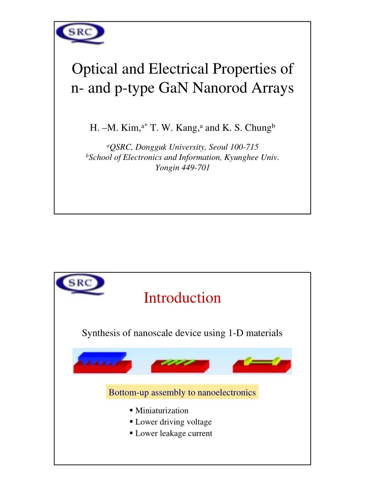
Optical and Electrical Properties of n- and p-type GaN Nanorod - PDF document
Optical and Electrical Properties of n- and p-type GaN Nanorod Arrays H. M. Kim, a* T. W. Kang, a and K. S. Chung b a QSRC, Dongguk University, Seoul 100-715 b School of Electronics and Information, Kyunghee Univ. Yongin 449-701 Introduction
Optical and Electrical Properties of n- and p-type GaN Nanorod Arrays H. –M. Kim, a* T. W. Kang, a and K. S. Chung b a QSRC, Dongguk University, Seoul 100-715 b School of Electronics and Information, Kyunghee Univ. Yongin 449-701 Introduction Synthesis of nanoscale device using 1-D materials Bottom-up assembly to nanoelectronics � Miniaturization � Lower driving voltage � Lower leakage current
GaN nanorods Growth • Growth conditions : Growth Temperature (T g ) = 450 ~ 550 ° C HCl = 30 ~ 150 sccm, N 2(HCl) = 300 ~ 2000 sccm NH 3 = 300 ~ 2000 sccm, N 2(NH3) = 300 ~ 2000 sccm N 2(main) = 3 ~ 5 slm, P tot = 1 atm • n, p-type GaN nanorods Growth Ga + N (+ Si ) Ga + N + Mg n-type p-type GaN nanorods FET Ti / Al (100 / 200nm) : n-type Ni / Au (100 / 200nm) : p-type 10 µ m SEM image of a GaN nanorod FET Schematic of a nanorod FET structure
I-V of GaN nanorods FET < n-type > n - channel Source Drain SiO 2 layer Si substrate Back gate + � Ohmic contact � Nanorods performed as a n - channel I-V data recorded on an 80 nm diameter n-type GaN nanorod I-V of GaN nanorods FET < p-type > p - channel Source Drain SiO 2 layer Si substrate Back gate - � Ohmic contact � Nanorods performed as a p - channel I-V data recorded on an 80 nm diameter p-type (Mg-doped) GaN nanorod
p-n Junction in Nanorods n-type growth p-type growth UV LEDs of GaN Nanorods (a) SEM image of a p–n junction within GaN nanorod with Ni/Au contact electrode for p-type and with Ti/Al contact electrode for n-type. Scale bars, 10 µ m. The diameter of the nanorod is 50 nm. The diameters of the nanorods used to make devices were in the range of 30–80 nm. (b) I–V behavior of n–n, p–p and p–n junctions, respectively. The blue and green curves correspond respectively to the I–V behavior of the individual n– and p–type nanorods. The red curve represents the I–V behavior of the GaN nanorod p–n junction. (c) Luminescence image of the light emitted from a forward–biased nanorod p–n junction at 3 V correspond to (a). Scale bar, 10 µ m. (d) Luminescence spectrum from the forward-biased p–n junction shown in (c). The spectrum peaks at 3.179 eV (390 nm). All data were recorded at room temperature in high–resolution SEM with a CL system.
Field Emission Displays of GaN Nanorods (a) Schematic structure of the GaN nanorods field emission displays. (b) Emission current of GaN nanorod as a function of electric fields. Inset corresponding Fowler–Nordheim (F–N) plot of GaN Nanorods, indicating a conventional field-emission mechanism. The emission current significantly deviated from F–N behavior in the high–field region. (c) Fluctuation of GaN nanorods field electron emitter, which was measured in a vacuum chamber and sealed GaN nanorods field electron emitter setup at constant voltage (electric field of 1.3 V/ µ m). (d) Anode image of field electron emission from “Q” character patterned GaN nanorods sample. Scale bar, 1 mm. Summary � n- and p-type GaN nanorods was directly grown by HVPE. � The p-n junction in the GaN nanorods was fabricated. � Nanoscale UV-LEDs were fabricated by using GaN nanorod. � GaN nanorods can be used to the display device such as FED.
Recommend
More recommend
Explore More Topics
Stay informed with curated content and fresh updates.

