Normal-Conducting Photoinjector for High Power CW FEL Sergey - PowerPoint PPT Presentation
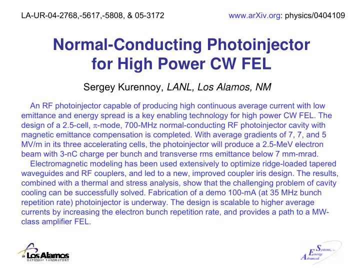
LA-UR-04-2768,-5617,-5808, & 05-3172 www.arXiv.org: physics/0404109 Normal-Conducting Photoinjector for High Power CW FEL Sergey Kurennoy, LANL, Los Alamos, NM An RF photoinjector capable of producing high continuous average current with low
LA-UR-04-2768,-5617,-5808, & 05-3172 www.arXiv.org: physics/0404109 Normal-Conducting Photoinjector for High Power CW FEL Sergey Kurennoy, LANL, Los Alamos, NM An RF photoinjector capable of producing high continuous average current with low emittance and energy spread is a key enabling technology for high power CW FEL. The design of a 2.5-cell, π -mode, 700-MHz normal-conducting RF photoinjector cavity with magnetic emittance compensation is completed. With average gradients of 7, 7, and 5 MV/m in its three accelerating cells, the photoinjector will produce a 2.5-MeV electron beam with 3-nC charge per bunch and transverse rms emittance below 7 mm-mrad. Electromagnetic modeling has been used extensively to optimize ridge-loaded tapered waveguides and RF couplers, and led to a new, improved coupler iris design. The results, combined with a thermal and stress analysis, show that the challenging problem of cavity cooling can be successfully solved. Fabrication of a demo 100-mA (at 35 MHz bunch repetition rate) photoinjector is underway. The design is scalable to higher average currents by increasing the electron bunch repetition rate, and provides a path to a MW- class amplifier FEL.
Normal-Conducting RF Photoinjector • Requirements and parameters: – CW, 700-MHz RF; emittance < 10 mm·mrad at the wiggler – 3 nC per bunch, 100 mA at 35-MHz bunch rep rate ( → 1 A) • Design: – split cavities: 2.5-cell PI (old 777 design: 7,7,7 MV/m, 2.70 MeV → new 775 design: 7,7,5 MV/m, 2.54 MeV) + booster (4 cells, 4.5 MV/m, 5.5 MeV) – PI: 2.5 cells, emittance-compensated, on-axis electric coupling – 100 mA: P w (668 kW) + P b (254 kW) → 1 A: 668 kW + 2540 kW • EM modeling: cavity, RF couplers, and ridge-loaded tapered waveguides • Beam dynamics – TS2 versus Parmela • Thermal & stress analysis, manufacturing → AES, Medford, NY CASA / Beam Physics Seminar, JLab. May 26, 2005 2
2.5-cell RF Photoinjector Cavity Magnets Vacuum plenum Cavity MAFIA model of 2.5-cell cavity with magnets and vacuum plenum CASA / Beam Physics Seminar, JLab. May 26, 2005 3
2.5-cell RF Photoinjector Cavity 2.5-cell PI with vacuum plenum – SF & MAFIA results CASA / Beam Physics Seminar, JLab. May 26, 2005 4
Normal-Conducting RF Photoinjector Cooling Photocathode plate Ridged tapered waveguides for RF power input 2.5-cell PI with emittance-compensating magnets (left) and vacuum plenum (right) CASA / Beam Physics Seminar, JLab. May 26, 2005 5
NC RF Photoinjector: Microwave Studio Modeling Photo- cathode position On-axis electric field for 0 18 MV/m 777(old) and 775 designs Electric field of π -mode in 2.5-cell cavity: E 0 =7 MV/m in cells 1&2, 5 MV/m in cell 3. CASA / Beam Physics Seminar, JLab. May 26, 2005 6
NC RF Photoinjector: Microwave Studio Modeling 43 W/cm 2 For comparison: in the old (777) design 75 W/cm 2 in 3 rd cell 103 W/cm 2 Power in the 775 design: P w = 668 kW versus P b = 254 kW for 100 mA, but 17.25 kA/m 0 P b = 2540 kW for 1 A Surface current distribution for the π -mode in 2.5-cell photoinjector cavity (775) CASA / Beam Physics Seminar, JLab. May 26, 2005 7
RF Power for NC Photoinjector • 922 kW of RF input power for 100 mA beam current: – CW, 700-MHz RF power is fed through two waveguides • Ridge-loaded tapered waveguides (RLWG) – Design is based on LEDA RFQ and SNS power couplers – Ridge profile is found by SF calculations for cross sections (LY), and checked using MicroWave Studio (MWS) 3-D calculations • “Dog-bone” shaped RF coupling irises Transition section from full-height WG1500 to half-height WG1500 Ridge-loaded tapered waveguide CASA / Beam Physics Seminar, JLab. May 26, 2005 8
EM Modeling of RF Coupler General layout of the model “Dog-bone” iris of RF couplers Half-height Ridge-loaded tapered WG 1500 waveguides for RF input RF coupler model. Tapered ridge-loaded waveguides are coupled to the 3 rd cell of photoinjector cavity (modeled here by a pillbox) via irises cut through thick walls. CASA / Beam Physics Seminar, JLab. May 26, 2005 9
EM Modeling of RF Coupler Details of coupler irises R 19 mm 2 ″ “Dog-bone” iris Ridge-loaded tapered Hole Ø 9.5 mm of RF couplers waveguide & iris RF coupler model. Details of coupler irises and ridge-loaded tapered waveguides. The wall thickness near the iris is 1.2 ″ , the iris gap width is 1.8 mm. CASA / Beam Physics Seminar, JLab. May 26, 2005 10
EM Modeling of RF Coupler Procedure + P P For 100 mA, the required WG-cavity coupling is β = = w b 1.38. c P w 2 ⎛ ⎞ H Q W For the pillbox model, the required coupling is β = β pb pb c ⎜ ⎟ . pb c ⎝ ⎠ W H Q pb c c 2 ⎛ ⎞ W Q H = = Then the required Q e for the model is pb ⎜ ⎟ c c Q 1933. ⎜ ⎟ β e W H ⎝ ⎠ c c pb We calculate Q e in the model directly using time-domain simulations with MicroWave Studio (MWS), and adjust the coupling. After that, again in MWS, an RF signal with a constant amplitude is fed into waveguides to find the match point ( P out = 0), and calculate the field and surface power distributions at the match. S.S. Kurennoy, L.M. Young. “RF Coupler for High-Power CW FEL Photoinjector”, PAC2003, p. 3515. CASA / Beam Physics Seminar, JLab. May 26, 2005 11
EM Modeling of RF Coupler: Time Domain (TD) MWS time-domain calculations: 1. Determine Q e 2. Find match point Match point for Amplitudes of: I beam = 100 mA: P out = 0 RF input signal Output signal Thermal test point: I beam = 0 P out = 0.025 P in CASA / Beam Physics Seminar, JLab. May 26, 2005 12
EM Modeling of RF Coupler − = + ≡ β From energy balance one can find power ratio P P P P P in out w b w ( ) 2 ⎛ ⎞ ⎛ ⎞ β β + + − 2 P 1 y 1 y 1 x ⎜ ⎟ = − α 1 where out ⎜ ⎟ = ⎜ 1 f , , f ( , ) x . β β ⎟ + ⎝ ⎠ P ⎜ 2 ⎟ y 1 y x in c c ⎝ ⎠ Coefficient 0< α <1 is the amplitude ratio of the input and reflected waves, 1- α <<1. For β = 1, β c = 1.38, ratio P out / P in ≈ 0.025, practically independent of value of α . 0.25 For α = 1, 0.2 (1-x) 2 /(1+x) 2 ; � P in α = 0.99; 0.15 P out α = 0.95; 0.1 α = 0.90. 0.05 • 0.5 0.75 1 1.25 1.5 1.75 Β � Β c CASA / Beam Physics Seminar, JLab. May 26, 2005 13
EM Modeling of RF Coupler: TD Results Maximal power density is 120 W/cm 2 at 461 kW RF input power per waveguide Regions with high power density are Fields values are for 0.5 W well localized → separate cooling RF input power and should be scaled by factor 960 Surface magnetic fields at the match point from MWS time-domain simulations CASA / Beam Physics Seminar, JLab. May 26, 2005 14
EM Modeling of RF Coupler: TD Results Maximal power density is 120 W/cm 2 at 461 kW RF input power per waveguide Fields values are for 0.5 W RF input power and should be scaled by factor 960 Surface currents near the irises at the match from MWS time-domain simulations CASA / Beam Physics Seminar, JLab. May 26, 2005 15
EM Modeling of RF Coupler: TD Results Maximal power density is 120 W/cm 2 at 342 kW RF input power per waveguide Max power density is the same as for the 100-mA match point Fields values are for 0.5 W RF input power and should be scaled by factor 827 Surface currents near the irises at thermal-test point (no beam, 2.5% reflection) CASA / Beam Physics Seminar, JLab. May 26, 2005 16
EM Modeling of RF Coupler: Eigensolver X-check Fields values should be Maximal power density 120 W/cm 2 scaled by factor 0.636 Surface currents from MWS eigensolver calculations (mesh 3.006M for 1/8) CASA / Beam Physics Seminar, JLab. May 26, 2005 17
EM Modeling of RF Coupler: Results for 775 MWS time domain MWS eigensolver Mesh, Max dP/ds , Mesh, Max dP/ds , Compare to 43 W/cm 2 K points W/cm 2 K points W/cm 2 at smooth wall in the 3 rd cell far from irises: 111 107 86 95 power ratio is < 2.8 → 111* 104* 201 109 field enhancement 312 120 due to irises is < 1.65 734 120 312* 119* 1539 122 760 114 3006 118 For 777 design max dP/ds was 760* 114* 220 W/cm 2 * W/o beam, 342 kW per WG (incl. 2.5% reflection) For reference: in the LEDA RFQ couplers max dP/ds ≈ 150 W/cm 2 , while the power ratio (max / smooth wall) was about 10 Maximal values of surface power density from MWS calculations CASA / Beam Physics Seminar, JLab. May 26, 2005 18
NC Photoinjector, RF Couplers : Summary • 100-mA operation of normal conducting photoinjector requires almost 1 MW of CW 700-MHz RF power that will be fed through two ridge-loaded tapered waveguides. • RF coupler design is based on LEDA RFQ and SNS couplers. The coupler-cavity system is modeled using a novel approach with direct MWS time-domain simulations. Results for the maximal power density are checked using eigensolvers. • The coupler design is optimized using 3-D EM modeling to reduce the maximal surface power density on the coupler irises: – Increased hole radius and wall thickness; blended iris edges; – Field enhancement is only 65% compared to smooth cavity walls. • In the 775 PI cavity, the max power density near the irises is only 15% higher than max in the smooth cavity. This design reduces stresses and facilitates cavity cooling. Thermal management is still challenging but feasible. • The PI cavity is being manufactured by AES. Its thermal tests with full RF load are scheduled at LANL (LEDA) in early 2006. CASA / Beam Physics Seminar, JLab. May 26, 2005 19
Recommend
More recommend
Explore More Topics
Stay informed with curated content and fresh updates.
