New and Emerging Technologies for Hadron Collider Detectors Julia - PowerPoint PPT Presentation
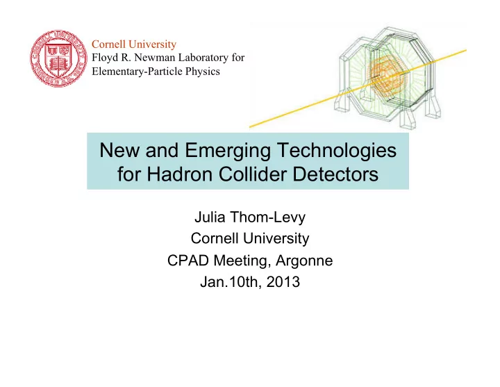
Cornell University Floyd R. Newman Laboratory for Elementary-Particle Physics New and Emerging Technologies for Hadron Collider Detectors Julia Thom-Levy Cornell University CPAD Meeting, Argonne Jan.10th, 2013 Large number of emerging
Cornell University Floyd R. Newman Laboratory for Elementary-Particle Physics New and Emerging Technologies for Hadron Collider Detectors Julia Thom-Levy Cornell University CPAD Meeting, Argonne Jan.10th, 2013
Large number of emerging technologies • Talk is supposed to focus on novel technology relevant to the EF, with longer time scale (10-15y) • Will take time, but have potential to meet the demands of future detectors in completely new ways – high resolution, high bandwidth, high rate – low power, low cost, low mass, large scale – complex functionality – radiation hardness • Have seen interesting talks about this already yesterday- – Pellin’s talk about ALD, transition edge detectors – Daniela’s talk on future instrumentation issues 2
My (incomplete) list : 1) Using recent “revolutions” in semiconductor technology • Vertical (3D) integration of sensors and electronics (Lipton,..) • SOI-based pixel detectors (Deptuch, Denes, Khalid,..) • Flexible and large area electronics (Forrest, PARC) • amorphous hydrogenated silicon deposited on readout (Jarron, talk in J) 2) Novel materials and emerging technologies • Gaseous proportional pixel detector (GridPix/Gossip) (vdGraaf) • SiPMs and other single soft photon detection (vdGraaf,…) • Atomic layer deposition (see plenary talk by Pellin on new materials) • New crystals for calorimetry using SiPMs (Para, Zhu..) • Water-based scintillators (Yeh, see talk in G) • Low-mass materials (Garcia, Haber,..,see talk by Cooper in session E) • Power delivery (Dhawan, see talk in E) • Large area pico-second photo detectors (Frisch, Wagner, ..Vav’ra talk in E) • Diamond detectors (Schnetzer, see talk in session E) • Superconducting Sensors (kinetic inductance, quantum-limited amplifiers) (Irvin in E) • … 3
It’s our charge to • catalog these topics and summarize – how they relate to the physics we want to do – What are pros and cons • Identify “high-impact, high-risk”, i.e. which ones to bet on – which ones may be unique and promise US leadership • Need to be careful to distinguish between “what we want” and “what we need”. 4
1) Recent revolutions in semiconductor technology • Breakthroughs in (nano)-fabrication – using novel materials like Ge, SiC, GaN, Diamond, carbon nanotubes, organic semiconductors as inks, … – structural engineering: SOI, MAPS,.., wafer thinning and bonding – implantation advances: multiple wells, pixel structure, charge storage and manipulation – can now build complex architectures: vertical integration of highly specialized layers • Goes hand-in-hand with new and sophisticated modeling and design tools – ASIC design – detailed semiconductor physics models • Very important: foundries now offer these specialized processes, and companies offer interconnect services – can now tailor devices to specific application, using large range of new technologies 5
Example: 3D Electronics • Industry and government initiatives to develop vertical integration, as it was recognized that scaling feature size would not extend Moore ’ s law beyond ~ 2020 • What is vertical integration: Optical Fiber In Optical Fiber Out – 2 or more layers ( “ tiers ” ) of active semiconductor devices that have been thinned, Opto Electronics bonded and vertically interconnected to form a monolithic circuit Digital layer Analog Layer • improve circuit performance. 50 um – reduce R, L, C for higher speed Sensor Layer – reduce chip I/O pads (less dead area) Designer’s Dream – technology of each layer can be separately optimized – reduce interconnect power and crosstalk – can increase complexity- more transistors per cm 2 – process now accessible commercially 6
Enabling key technologies WB/BB pad – Wafer bonding (oxide bonding, adhesive bonding, TSV eutectic bonding, Cu-Cu bonding,..) • Allows for sensor/readout integration to form a monolithic unit Inter-tier bond pads – Etching and processing of precision vias in silicon 1 st wafer • Fine pitch interconnect Tezzaron 2-tier wafer • 3D and edgeless sensor technology – Precision alignment (<1 µ m) – Wafer thinning (<25 µ m) • Low mass sensors • Backside processing • New ways to think electronics/detector 7 MIT-LL Three tier SOI wafer integration
3D Applications • We are just at the beginning of exploring 3D • FNAL Tezzaron/Chartered + KEK/OKI + Future – 3D sensors (S. Parker et al) – ILC Vertex VIP2 Chip – LHC track trigger sensor – X-ray imaging with time tag Back Side Metal (thinned wafer) SuperContact – CMOS pixel with PMOS devices Tier 1 placed on the tier without sensing diodes M1 M2 M3 M4 M5 – ATLAS pixel chip size reduction Bond Interface M6 M6 M5 M4 – Super B vertex M3 M2 Tier 2 M1 – X-ray imaging SuperContact – B factory Vertex – CMOS/CCD integration – SiPM with per pixel digital readout – 3D associative memories for triggering 8
3D for CMS Track Trigger sensor FNAL, Cornell, Davis,… • CMS Track trigger – need to correlate hits from 2 layers separated by ~mm to filter on p t > 2-3 GeV sensor – 3D allows connection of chip to both top and bottom sensors space by low density Etched via through 0.5mm silicon interposer interposer – correlations formed locally by bottom chip, saving power, complexity • First demonstrator unit close to done Long Strip Sensors bump bonding Interposer 3D chip w/TSVs Fusion bonding Short Strip Sensors 9
Track Trigger Collaboration Serial RO of all top & bottom strips + coincidence Bump-bonding , UC Davis Interposer: Cornell, AllVia, Tezzaron Sensors / edgeless sensors: IC design: BNL, VTT LBNL 3D ASICs with TSVs: Tezzaron DBI/fusion bonding: Ziptronix, T-micro, RTI 10
First readout chip “tiers” from the 3D multiproject run were received in September 2011: • Wafer was back-thinned, and back Al pads were deposited, then singulated and distributed 3D ¡Multiproject ¡Reticule ¡ 11
Testing of first stacked devices (VICTR chip) Some 3D circuits performed properly, but problems with pixel interconnects. Cause: substantial misalignment of top and bottom layers. Problem fixed now • misalignment of bonding interface M6 top M6 bot Testing the VICTR chip at FNAL and CU: time walk measurements, threshold scans and tuning, investigating crosstalk, etc 12 • SEM picture courtesy of P. Siddons BNL
Towards larger area modules with 3D • Size of 3D devices determined by reticule size – Sub-micron CMOS electronics dictates ~2x3 cm • If we want to bond to a larger area sensor there is a very serious issue of yield (i.e. many small chips bonded to large sensor) – Smaller sensors are problematic because saw edges cause leakage currents- active area constrained to distance from the edge 2-3 times the thickness, causing dead area Eraenen, Kalliopuska et al,NIM A 607 (2009) • How to make larger area fully active 85-88 modules? active edge sensors Ion etching can produce an “ atomically smooth ” edge – small leakage and sensitive to within a few microns of the edge (compare to 3x thickness of conventional sensors due to leakage currents) (see talk by C.Kenney in session E) 13
Enabling innovative designs with simulation • capital investment for fabrication of prototypes is large • modern sophisticated simulations allow us to “try out” various new designs to explore electric properties in detail (IV curves, breakdown, aging,…) • example: commercial 3D TCAD process simulation software used to study new edgeless strip sensors and fine-tune geometry before next submission – software license inexpensive at Universities (e.g. Cornell) Work by postdoc W.Hopkins, CU Layout of strip sensor Showing charge density due to 3.5GeV muon hitting near the edge- study charge collection and edge effects. Leakage currents for different 14 strip distances from the edge (in micron)
Silicon-on-Insulator (SOI) development • An SOI device contains a thin (200nm) silicon device layer mounted on a “ handle ” wafer. Can be a high resistivity detector. • first studied in 1993 by CERN/CPPM/IMEC • 2000s Crakow group in-house fabrication • FNAL SBIR studies with American Semiconductor dual gate transistors • KEK-organized multiproject runs with OKI • excellent foundry-FNAL communication • physical models to understand digital-analog crosstalk • Cornell: device simulation • Parallel work on thinning/backside process • qualification of thinning process • development of laser anneal process (FNAL-Cornell) 15
Ongoing development of SOI technology for HEP • More complex architectures, e.g. nested well implants for SOI and CMOS devices to shield layers from each other (FNAL: Deptuch, Denes,..) • Development of pixel electronics (Monolithic Active pixel Matrix with Binary cOunters) at FNAL using fully depleted CMOS SOI 0.2 µm process as the base • Close to a fully functional detector for application to HEP – So far generic R&D • Many good features- low power, large range of operating temperature, low single event effect, vertical integration, ... 16
Recommend
More recommend
Explore More Topics
Stay informed with curated content and fresh updates.
