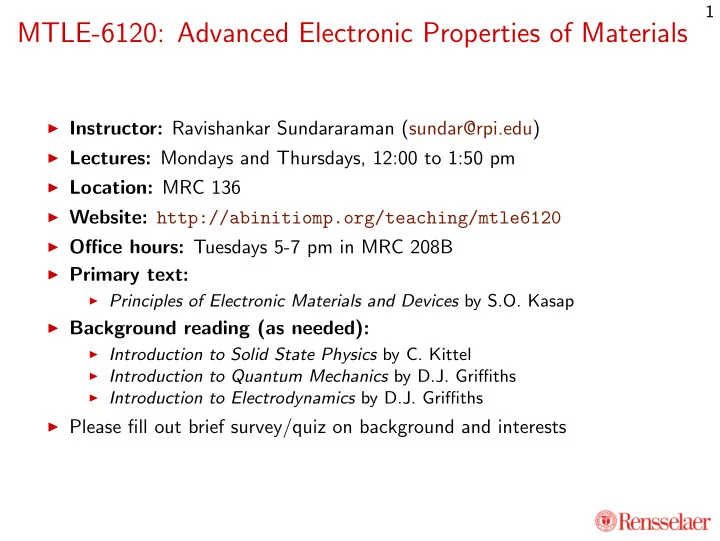

1 MTLE-6120: Advanced Electronic Properties of Materials ◮ Instructor: Ravishankar Sundararaman (sundar@rpi.edu) ◮ Lectures: Mondays and Thursdays, 12:00 to 1:50 pm ◮ Location: MRC 136 ◮ Website: http://abinitiomp.org/teaching/mtle6120 ◮ Office hours: Tuesdays 5-7 pm in MRC 208B ◮ Primary text: ◮ Principles of Electronic Materials and Devices by S.O. Kasap ◮ Background reading (as needed): ◮ Introduction to Solid State Physics by C. Kittel ◮ Introduction to Quantum Mechanics by D.J. Griffiths ◮ Introduction to Electrodynamics by D.J. Griffiths ◮ Please fill out brief survey/quiz on background and interests
2 Topics ◮ Theoretical background ◮ Maxwell’s equations in materials ◮ Classical Drude theory of conduction ◮ Review of basic quantum mechanics ◮ Atoms, many-electron theories and the periodic table ◮ Quantum kinetics: Fermi’s Golden rule ◮ Band theory of solids ◮ Material properties ◮ Fermi theory of metals ◮ Electron transport: phonons and electron-phonon interactions ◮ Intrinsic and extrinsic semiconductors ◮ Insulating materials: dielectrics, ferroelectrics, piezoelectrics etc. ◮ Magnetism: dia-, para- and ferro-magnetism, hysteresis ◮ Superconductivity ◮ Optical properties: absorption, emission, luminescence, fluorescence, lasing ◮ Two-dimensional materials ◮ Electrical and optical properties of polymers
3 Topics (contd.) ◮ Interface properties ◮ Metal-vacuum interfaces: thermionic emission ◮ Fowler-Nordheim tunneling: field emission ◮ Metal-metal junctions: Seebeck effect, thermocouples, Peltier effect ◮ Metal-semiconductor Schottky junctions; Fermi-level pinning ◮ Semiconductor p-n junction diodes ◮ Light-emitting diodes, photodetectors and semiconductor lasers ◮ Technological applications ◮ Semiconductor transistors for logic and memory ◮ Magnetic storage devices: giant magnetoresistance ◮ Solid-liquid interfaces: photocatalysis, supercapacitors
4 Learning outcomes ◮ Understand how the physics of electrons in materials results in a variety of electronic, magnetic and optical properties of materials ◮ Understand how these properties are exploited and optimized for in technological applications ◮ Navigate literature in active areas of research in electronic, magnetic or optical materials
5 Assessment ◮ 20% : Weekly quizzes in Thursday classes based on most-recent lectures and homework; one lowest score not counted ◮ 20% : In-class midterm examination on Feb 26, which along with all previous homeworks will be used to provide you with performance feedback by Feb 28 ◮ 10% : Short oral presentation on an area of active research in electronic, optical or magnetic materials in the last few classes (April 23 and 26) ◮ 40% : Final examination on the last day of classes (Apr 30) ◮ 10% : Participation in class by asking questions and contributing to discussions
6 Academic integrity Student-teacher relationships are built on trust. For example, students must trust that teachers have made appropriate decisions about the structure and content of the courses they teach, and teachers must trust that the assignments that stu- dents turn in are their own. Acts that violate this trust undermine the educational process. The Rensselaer Handbook of Student Rights and Responsibilities and The Graduate Student Supplement define various forms of Academic Dishonesty and you should make yourself familiar with these. ◮ Homework: discussions and team work encouraged (not for grade) ◮ Quizzes / exams: books and printed notes allowed; no discussions ◮ First violation: zero score on that assignment ◮ Second violation: F grade on course If you have any question concerning this policy, please ask for clarification.
7 Fastest advancing technologies ◮ Computer processors ◮ Magnetic storage (hard drives) ◮ Solid-state storage (flash memory) ◮ Optical communications ◮ Photovoltaics (solar cells) Spolier: they all involve electronic, magnetic and optical materials
8 Moore’s law: CMOS transistor count Source: Wgsimon/Wikimedia commons
9 Moore’s law: computation rate per cost Where would you mark yourself on this plot? Source: S. Jurveston/Wikimedia commons
10 Moore’s law: storage aereal density Source: Adv. Tribol. 2013 , 521086 (2013)
11 Keck’s law: fiber optic communication rate Source: J Hecht on IEEE spectrum, 26 Jan 2016
12 Photovoltaic efficiencies Equally impressive: efficiency is much harder than device scaling Source: S. Kurtz and D. Levi, NREL
13 Goals of this course ◮ Physical laws → material properties ◮ Material properties → device functionality ◮ Device functionality → technologies (briefly)
Recommend
More recommend