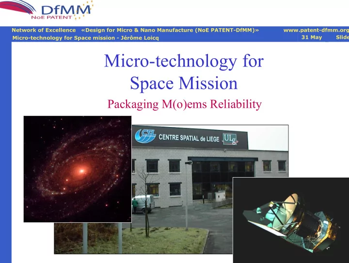

Network of Excellence «Design for Micro & Nano Manufacture (NoE PATENT-DfMM)» www.patent-dfmm.org 31 May Slide Micro-technology for Space mission - Jérôme Loicq Micro-technology for Space Mission Packaging M(o)ems Reliability
Plan Network of Excellence «Design for Micro & Nano Manufacture (NoE PATENT-DfMM)» www.patent-dfmm.org 31 May Slide Micro-technology for Space mission - Jérôme Loicq • Introduction • Space environment • Definition • Problems evaluation • Reliable materials for space • Solution from space heritage • Space design guidelines • Space qualification for Micro technology • Downscaling • James Webb Space Telescope • Test-sequences and CSL facilities • Conclusions
Introduction Network of Excellence «Design for Micro & Nano Manufacture (NoE PATENT-DfMM)» www.patent-dfmm.org 31 May Slide Micro-technology for Space mission - Jérôme Loicq • Why space mission can be interested with micro-technology? • Size, mass, power consumption are constrained in S.M. • Launching (10 000 to 100 000$/kg) • Increase interest to “nano-satellite” » Network of very small satellites
Space environment requirements Network of Excellence «Design for Micro & Nano Manufacture (NoE PATENT-DfMM)» www.patent-dfmm.org 31 May Slide Micro-technology for Space mission - Jérôme Loicq • Thermal environment (-150°C to 150°C) • Vacuum conditions induce outgassing and contamination • Energetic charged particles and plasma • Atomic oxygen • Micrometeoroid and Space debris • Vibration
Failure mechanism induced in space environment Network of Excellence «Design for Micro & Nano Manufacture (NoE PATENT-DfMM)» www.patent-dfmm.org 31 May Slide Micro-technology for Space mission - Jérôme Loicq • Temperature cycling (between -150 to +150°C) – Fatigue • decreases the performance of lubricant • decreases the life-time of thermal control fluids • induces vibration of solar panel and destabilization of spacecraft – Internal stress • poor Thermal Expansion matching => internal stress – Metal packaging • CTE 10 times greater than silicon =>fracturing of the substrate – Semiconductors • modification of mechanical, charge transport properties
Failure mechanism induced in space environment Network of Excellence «Design for Micro & Nano Manufacture (NoE PATENT-DfMM)» www.patent-dfmm.org 31 May Slide Micro-technology for Space mission - Jérôme Loicq • Vacuum effects – mechanical trouble • especially for movable sections • cold welding: pieces manufactured in the same metal are joined together – contamination by outgassing (release of a gas trapped or frozen in some materials) • diminishing performance of optical elements • off-axis radiation scattering • increasing mirror scattering – contamination by sublimation or vaporization • loss of structural material
Contamination Network of Excellence «Design for Micro & Nano Manufacture (NoE PATENT-DfMM)» www.patent-dfmm.org 31 May Slide Micro-technology for Space mission - Jérôme Loicq • Contamination understanding: • Outgassing from warm surface – Condensation on colder surface – Contaminant layer is fixed with UV radiation • Otherwise, not permanently attached – Contaminant darkens with UV (optical loss is cumulating absorptivity and layer thickness increases) – Heating the surface vaporizes the contaminant (only when not permanently attached by UV)
Failure mechanism induced in space environment Network of Excellence «Design for Micro & Nano Manufacture (NoE PATENT-DfMM)» www.patent-dfmm.org 31 May Slide Micro-technology for Space mission - Jérôme Loicq • Vibration (launch process) – surface adhesion – fracturing Cracks in single crystal silicon support beams caused by vibrations induced by a launch simulation
Failure mechanism induced in space environment Network of Excellence «Design for Micro & Nano Manufacture (NoE PATENT-DfMM)» www.patent-dfmm.org 31 May Slide Micro-technology for Space mission - Jérôme Loicq • Shock (during launch or transient mission phase) – high stress • buckling of long and slender structure • plastic deformation of structures • fracture in brittle components – high acceleration • vibration of relays • slip of the potentiometers • loss of bolts – excessive displacement • broken solder joints • cracked PC boards and wave guides – shock environment • electrical malfunctions in capacitors, crystal oscillators...
Failure mechanism induced in space environment Network of Excellence «Design for Micro & Nano Manufacture (NoE PATENT-DfMM)» www.patent-dfmm.org 31 May Slide 1 Micro-technology for Space mission - Jérôme Loicq • Atomic oxygen – formation of insulation compound at surfaces =>increase of power loss • Charged particles – electrostatic discharge with catastrophic effects on electronics circuits • Space debris – the impact of fast moving particles can vaporize of fragments pieces
Failure mechanism induced in space environment Network of Excellence «Design for Micro & Nano Manufacture (NoE PATENT-DfMM)» www.patent-dfmm.org 31 May Slide 1 Micro-technology for Space mission - Jérôme Loicq • Radiation – Ionization • creation of electron hole pairs within dielectric =>flatband threshold voltage shift, surface leakage current,... – Displacement • atom in crystal lattice are displaced by energetic particles => thermal dark current, loss in charge transfer efficiency, increased current in reverse biased junction... – Single event effect • interaction of single particle (p+, e-,…) with semi conductor => dark current generation centers
Radiation Network of Excellence «Design for Micro & Nano Manufacture (NoE PATENT-DfMM)» www.patent-dfmm.org 31 May Slide 1 Micro-technology for Space mission - Jérôme Loicq • Experience of Space Solar cell • The best semiconductors materials:SiC, GaAs, InP and combinations » lowest reactivity with high energy radiation • Solar cell packaging – Borosilicate glass with a nominal 5% of cerium dioxide . This ceria stabilizes the glass preventing the formation of color centers under electron and proton irradiation. • Optical material • Radiation induce Color center � Reduction of optical transmission properties
Space design guidelines Network of Excellence «Design for Micro & Nano Manufacture (NoE PATENT-DfMM)» www.patent-dfmm.org 31 May Slide 1 Micro-technology for Space mission - Jérôme Loicq Material selection: CTE mismatch should be avoid, radiation shielding foreseen and contamination understanding Venting holes: the outgassing products are guided through venting holes (ie Multi Layer Insulator). The outgassing is decreased by performing a prior bake out of by flushing with dry nitrogen during storage. Cold traps: collect contaminants and depend on the sticking coefficient (ie at 120K 100% of water molecules stick Chemical getters: trap particular molecules, especially water; zeolith getter are also successfully used Heaters: if contamination is not fixed to the surface (by UV cross-linking), active heating may decontaminate (but require hit level of power consumption)
Example of contamination Network of Excellence «Design for Micro & Nano Manufacture (NoE PATENT-DfMM)» www.patent-dfmm.org 31 May Slide 1 Micro-technology for Space mission - Jérôme Loicq • Space Heritage: EIT (SOHO) – Loss related to ice contamination on CCD surface – Heating (~1 day) retrieves the sensitivity by sublimation – No venting holes in the vicinity: ice re-condensing – Periodic cleaning – Partial recovering only (other aging effects)
Downscaling Network of Excellence «Design for Micro & Nano Manufacture (NoE PATENT-DfMM)» www.patent-dfmm.org 31 May Slide 1 Micro-technology for Space mission - Jérôme Loicq • Package sealing: Hermetic or not hermetic? – Sealing protects from contamination and moisture from the outside world • During space mission, hermetic is not required (vacuum) • During AIT: hermetic is the best but flushing with dry nitrogen is a alternative solution – Sealing confines potential contamination inside the MOEMS • Venting holes in the vicinity of outgassing surface reduces the inner contamination vapor • Heaters could help vaporization on contaminant (see EIT)
Downscaling Network of Excellence «Design for Micro & Nano Manufacture (NoE PATENT-DfMM)» www.patent-dfmm.org 31 May Slide 1 Micro-technology for Space mission - Jérôme Loicq • Example: James Webb Space Telescope (JWST) – NIRSpec: IR spectrograph with MOEMMicro Mirror Array (MMA) Micro Shutter Array(MSA) MSA is finally selected for maturity reason...
Recommend
More recommend