Maximalist Cryptography and Computation on the WISP UHF RFID Tag - PDF document
Maximalist Cryptography and Computation on the WISP UHF RFID Tag Hee-Jin Chae 1 , Daniel J. Yeager 2 , Joshua R. Smith 2 , and Kevin Fu 1 1 University of Massachusetts, Amherst, MA, USA, { chae, kevinfu } @cs.umass.edu 2 Intel Research Seattle,
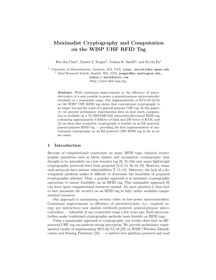
Maximalist Cryptography and Computation on the WISP UHF RFID Tag Hee-Jin Chae 1 , Daniel J. Yeager 2 , Joshua R. Smith 2 , and Kevin Fu 1 1 University of Massachusetts, Amherst, MA, USA, { chae, kevinfu } @cs.umass.edu 2 Intel Research Seattle, Seattle, WA, USA, yeagerd@ee.washington.edu, Joshua.r.smith@intel.com http://www.rfid-cusp.org/ Abstract. With continuous improvements in the efficiency of micro- electronics, it is now possible to power a general-purpose microcontroller wirelessly at a reasonable range. Our implementation of RC5-32/12/16 on the WISP UHF RFID tag shows that conventional cryptography is no longer beyond the reach of a general-purpose UHF tag. In this paper, (1) we provide preliminary experimental data on how much computa- tion is available on a TI MSP430F1232 microcontroller-based RFID tag containing approximately 8 KBytes of flash and 256 bytes of RAM, and (2) we show that symmetric cryptography is feasible on an RF-powered, general-purpose RFID tag — providing the first implementation of con- ventional cryptography on an RF-powered UHF RFID tag as far as we are aware. 1 Introduction Because of computational constraints on many RFID tags, classical crypto- graphic primitives such as block ciphers and asymmetric cryptography were thought to be unrealistic on a low-resource tag [9]. To this end, many lightweight cryptographic protocols have been proposed [5, 6, 14–16,18, 19]. However, many such protocols have serious vulnerabilities [7, 11, 12]. Moreover, the lack of a de- velopment platform makes it difficult to determine the feasibility of proposed cryptographic schemes. Thus, a popular approach is to minimize cryptographic operations to ensure feasibility on an RFID tag. This minimalist approach [9] can leave spare computational resources unused. An open question is then how to best maximize the security on an RFID tag to fully utilize available compu- tational resources. Our approach to maximizing security relies on low-power microcontrollers. Continuous improvements in efficiency of microelectronics (i.e., required en- ergy per instruction) now enables wirelessly-powered, general-purpose micro- controllers — infeasible at any reasonable range a few years ago. Such microcon- trollers make traditional cryptographic methods more feasible on RFID tags. Using a maximalist approach to cryptography, our results show that an RF- powered UHF tag can perform strong encryption. We provide preliminary exper- imental results of implementing RC5-32/12/16 [22] on WISP (Wireless Identifi- cation and Sensing Platform) [24] — a battery-free platform powered and read
Fig. 1. WISP [24, 23] is a batteryless, microcontroller-based UHF tag that implements RFID protocols in software. WISP uses a TI MSP430 microcontroller and minimal analog circuitry to function as a UHF RFID tag. by a standards compliant UHF RFID reader running the EPC Class 1 Gen 1 protocol. Our contributions include: 1. We provide preliminary experimental data on how much computation is available on a microcontroller-based RFID tag. 2. We show that symmetric cryptography is feasible on an RF-powered, general- purpose RFID tag. To the best of our knowledge, this is the first implemen- tation of conventional cryptography on an RF-powered UHF RFID tag. 2 Background on WISP Architecture This section provides a condensed background on the WISP, more fully described in [24, 23]. The WISP and its block diagram appear in Fig. 1. An antenna and impedance matching circuit precede the analog front end. The power harvester block rectifies incoming RF energy into DC voltage to power the system. The demodulator follows the envelope of the RF carrier wave to extract the Am- plitude Shift Keyed (ASK) data. This extracted baseband waveform is read by the MSP430 microcontroller to receive downlink data from the reader. Uplink data is sent via the modulator circuit, which functions by changing the antenna impedance. The WISP is made of a two layer FR4 PCB with components limited to the top side. A dipole antenna made of 22 gauge (0.6mm diameter) copper magnet wire is visible. Small header pins expose all ports of the microcontroller for expansion to daughter boards, external sensors and peripherals. Analog Front End and Tuning. Due to the relatively high power consumption of WISP, its rectifier is designed to supply more current than ordinary tags. This circuit is excited by commercial, EPC Class 1 Generation 1 compliant readers operating at 902-928 MHz with an allowable transmission power of 4 W EIRP (Effective Isotropic Radiated Power). Efficient conversion of the incoming RF energy to DC power for the tag maximizes range. A matching network provides maximum power transfer from the antenna to the rectifier, and a 5 stage voltage doubling circuit converts the
incoming power to voltage. Low threshold RF Schottky diodes maximize the voltage output of the rectifier. Finally, this rectified DC voltage is stored in a large capacitor and supplied to a 1.8 V regulator to power the WISP. Demodulation and Modulation. To encode reader-to-tag data, the reader amplitude- modulates the 915MHz RF carrier wave it emits. Normally the carrier waveform remains at a constant amplitude; when bits are transmitted, the amplitude of the carrier drops to approximately ten percent of its normal value. The duration of the low “break” indicates a logical “one” or a “zero.” A short break (1.78 uS) indicates a “zero,” and a long break (5.34 uS) indicates a “one.” To decode this data, the RF signal is fed through a small (two stage) voltage doubling rectifier in parallel with the main (five stage) harvester. We call the two stage harvester the “mini-harvester.” The time constant of the mini-harvester is much smaller than that of the main harvester, allowing it to track the dynamic range of the incoming bits. The first two voltage doubling stages of the mini-harvester, in conjunction with a lowpass filter, effectively demodulate the 915MHz carrier, and leave a baseband data signal on the order of 70kHz. A final “extra” diode performs an additional rectification step, removing the 70kHz data signal and leaving a slowly varying average power level (i.e., just fast enough so that it can change on the timescale that the tag moves in space, say 10Hz) that provides a dynamic reference for bit detection. The 70kHz data signal is fed through a Schmitt trigger inverter that thresh- olds this waveform to remove noise and glitches. Finally, a level shifter converts the relative magnitude of the incoming data waveform into a 1.8 V logic level for the MSP430. The slowly varying average power signal serves as the power supply for the Schmitt trigger and level shifter. RFID tags do not actively transmit radio signals. Instead they modulate the impedance of their antenna which causes a change in the amount of energy re- flected back to the reader. This modulated reflection is typically called backscat- ter radiation. In order to change the impedance of the antenna, a transistor is placed between the two branches of the dipole antenna. When the transistor conducts current, it short circuits the two branches of the antenna together, changing the antenna impedance; in the non-conducting state, the transistor has no effect on the antenna, and thus the power harvesting and data downlink functions occur as if it were not present. This impedance modulation is cur- rently implemented with a 5GHz RF bipolar junction transistor which allows for effective shunting of the 915MHz carrier wave. Digital section and power conditioning. The WISP’s general-purpose compu- tation capabilities are provided by an ultra low power microcontroller, the TI MSP430F1232. This 16-bit device has just over 8 KBytes of flash memory, 256 bytes of RAM and a 10-bit, 200kilo-samples-per-second Analog to Digital Con- verter (ADC). It can run at 8MHz with a 3.3 V supply voltage, 6MHz with a 3.0 V supply, and 4Mhz with a 1.8 V supply. To erase and write to flash memory, a minimum 2.7 V supply is required. In this application, we used a 3.0 V supply because a suitable ultra-low quiescent current 2.7 V regulator was not available.
Recommend
More recommend
Explore More Topics
Stay informed with curated content and fresh updates.
