LLCD will be the first high-rate space laser communications system - PowerPoint PPT Presentation
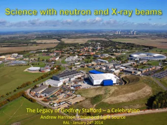
LLCD will be the first high-rate space laser communications system that can be operated over a range ten times larger than the near-Earth ranges that have been demonstrated to date. from http://esc.gsfc.nasa.gov/267/271.html, enabled by
“LLCD will be the first high-rate space laser communications system that can be operated over a range ten times larger than the near-Earth ranges that have been demonstrated to date.” from http://esc.gsfc.nasa.gov/267/271.html, enabled by nanowire detectors developed at MIT Lincoln Laboratory in collaboration with MIT campus.
VLSI Circuit Evaluation snspd ⦿ VLSI circuit imaging and debugging ⦿ SNSPD enables performance advances Image courtesy of DCG Systems Collaboration between BU, DCG Systems, IBM, Photonspot, funded by IARPA 15-06-12-washington-italy-meeting4
Characteristics of Photon Detectors • Efficiency incident photons with hν no signal voltage time • Reset time incident photons blocked by earlier signal time • Jitter varying delay between photons and signals time t 1 t 2 t 3 • Dark count rate voltage pulses with no corresponding photon time 5 2016-03-30-vancouver-ubc-5
4 nm Niobium nitride < 100 nm
resistive R T superconducting critical temperature, T c
I resistive critical current, I c bias point V superconducting
DETECT.SNSPD Calandri et al., Appl. Phys. Lett. , 109 (15) 152601( 2016). Korzh et al. , 1804.06839 With JPL and NIST
ħω Ch2 t 0 l /2 x - l /2 Ch1 t 1 t 2 t 0 - l /2 l /2 Position on wire
• A typical nanowire transmission line DETECT.SNSPD CPW, 300 nm center conductor width, ~ 5nm thick NbN 3µm gap, SiO2 on Si substrate SiO 2 300 nm Signal speed ~2% c Si Zhao et al. Nat. Photonics 11, 247 (2017) Au Microstrip, 300 nm width SiO 2 NbN AlN on Al 2 O 3 substrate 450 nm AlN Signal speed 1.6% c Al 2 O 3 Zhu et al. Nat. Nanotech. 13, 596 (2018) Au NbN CPW with top ground, 200 nm width, SiO 2 Si 1µm gap, 450 nm spacer, SOI SiO 2 substrate Signal speed 0.87% c Zhu et al. (2018), unpublished Si The group velocity can be further reduced by using high-index dielectric materials In collaboration with Daniel Santavicca (UNF )
μ μ
Two connectors for one imager (>500 pixels)
16 two-photon firing events among 50,000 photon detection events (flood illumination over the entire area) 16 two photon detection events voltage (V) time (ns)
75 nm
Large-area WSi SNSPD
Robert Lasenby Stanford
● Angle Velasco (JPL) ● Brian Noble (UNF) ● Andrew Beyer (JPL) ● William Strickland (UNF) ● Jason Allmaras (JPL) ● Edward Ramirez (JPL)
taper taper 14 mm 3 mm 1 mm The first transmitted pulses
μ μ
μ μ
μ μ
Recommend
More recommend
Explore More Topics
Stay informed with curated content and fresh updates.
