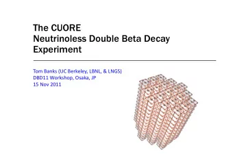
Large Area Plasma Enhanced Chemical Vapor Deposition of - PowerPoint PPT Presentation
Large Area Plasma Enhanced Chemical Vapor Deposition of Nanocrystalline Graphite on Insulator for Electronic Device Application Marek E. Schmidt 1) , Cigang Xu 2) , Mike Cooke 2) , Hiroshi Mizuta 1) , and Harold M. H. Chong 1) 1 Nano Research
Large Area Plasma ‐ Enhanced Chemical Vapor Deposition of Nanocrystalline Graphite on Insulator for Electronic Device Application Marek E. Schmidt 1) , Cigang Xu 2) , Mike Cooke 2) , Hiroshi Mizuta 1) , and Harold M. H. Chong 1) 1 Nano Research Group, School of Electronics and Computer Science, University of Southampton, UK 2 Oxford Instruments Plasma Technology, Bristol, UK 11 th April 2012
Outline Outline • Why PECVD for graphene deposition? • PECVD system and deposition • Nanocrystalline graphite (NCG) • Device fabrication • Conclusion
Why PECVD for graphene growth? Comparison of methods for growth of graphene Method Advantage Disadvantage Exfoliation from Use adhesive tape to Highest quality Random (shape, size, graphite peel graphene from Simple location) HOPG Does not scale Epitaxial growth on Anneal SiC (1200 – Good Control over Expensive substrates SiC 1500 ° C) number of layers High temperature � Si sublimation Large domains Surface steps Catalytic growth on Heat catalyst film and No limit of substrate Requires graphene metal supply hydrocarbon size transfer for electronic (CVD: 530 – 1000 ° C; Low temperature application SWP ‐ CVD: 300 ° C) Research into growth methods not exhausted •
PECVD deposition • PECVD in use for large ‐ area uniform film deposition • Different plasma ‐ enhanced CVD methods for graphene or graphene ‐ like film deposition reported • Remote PECVD [1] � Custom built/modified equipment • Surface wave PECVD [2] � On metal, requires transfer • Evaluate the PECVD route further [1] L. Zhang et al., Nano Research , vol. 4, no. 3, pp. 315–321, 2010. [2] J. Kim et al., Applied Physics Letters , vol. 98, no. 9, p. 091502–091502–3, 2011
Chemistry and PECVD System • Carbon source (CH 4 ) � CH x , C 2 H y , C 3 H z , H • Chemical binding followed by hydrogen desorption • PECVD system used • Oxford Instruments Nanofab 1000 Agile • 200 mm substrates, parallel plate configuration www.oxford-instruments.com
Deposition Process • Si wafer with 240 nm thermal oxide 1. Heat ‐ up from loading to processing temperature 2. Hydrogen pre ‐ treatment 3. PECVD deposition 4. Cool ‐ down and unload (step durations are typical values)
Deposition uniformity • 15 minutes, 900 ° C, 100 W RF, 90 sccm H 2 , 72 sccm CH 4 � 30 ‐ 37 nm thickness 25% 9% 150 mm (6”) substrate Ellipsometer thickness mapping
Raman 532 nm • Deposited films exhibit distinct D ( 1350 cm ‐ 1 ), G ( 1600 cm ‐ 1 ) and broad 2D ( 2700 cm ‐ 1 ) peaks • I (D)/ I (G) = 2.06 • Film described before [3] G ‐ peak position unaffected by λ (1600 cm ‐ 1 ) 1. 2. I (D)/ I (G) ≈ 2 � Nanocrystalline graphite [3] A. C. Ferrari and J. Robertson, Phil. Trans. R. Soc. A 362 (2004), pp 2477–2512
Nanocrystalline graphite • NCG is a film with crystalline (“graphene”) domains in random orientation • Size of crystalline domains L a can be estimated from I (D)/ I (G) ratio [4] λ I ( D ) C ( ) = I ( G ) L a • Our films L a = 2.2 to 2.7 nm SEM of NCG surface [4] A. C. Ferrari and J. Robertson, Physical Review B, 61(20) (2000), 14095
Other deposition conditions 532 nm 17% 8% Raman map 19% 9%
Device fabrication • Contacted NCG strips fabricated NCG 1. Thermally oxidized c ‐ Si substrate with NCG film resist 2. Lithography SiO 2 3. Oxygen-based dry etch of NCG and resist strip Ti/Au 4. Ti/Au contact patterning by lift-off
Resistivity • Fabricated devices ρ = 0.029 Ω cm • Van der Pauw ρ = 0.012 Ω cm
Film transparency • NCG deposited on quartz and sapphire • Optical transmission measured 6 nm on quartz 15 nm on sapphire 15 nm on quartz • 85% transparency @ 13 k Ω /sq for 6 nm film on quartz glass
Conclusion • Demonstrated large ‐ area, meta ‐ free PECVD of nanocrystalline graphite • Uniform NCG coverage over 150 mm substrates • Substrate size not limited • Sheet resistance in k Ω /sq range • NCG optical transparency > 85% • NCG can be easily patterned and contacted • Potentially usable for transparent electrodes
Growth comparison Lets look at the comparison again Method Advantage Disadvantage Exfoliation from Use adhesive tape to Highest quality Random (shape, size, graphite peel graphene from Simple location) HOPG Does not scale Epitaxial growth on SiC Anneal SiC (1200 – Good Control over Expensive substrates 1500 ° C) number of layers High temperature � Si sublimation Large domains Surface steps Catalytic growth on Heat catalyst film and No limit of substrate Requires graphene metal supply hydrocarbon size transfer for electronic (CVD: 530 – 1000 ° C; Low temperature application SWP ‐ CVD: 300 ° C) Plasma assisted Substrate exposed to Metal ‐ free ? deposition on insulator carbon plasma Large ‐ area (including this work) Directly on insulator
Acknowledgements • Financial support: University of Southampton, School of Electronics and Computer Science Scholarship • Fabrication: Southampton Nanofabrication Centre Dr. Owain Clarke
Thank you for your attention
Recommend
More recommend
Explore More Topics
Stay informed with curated content and fresh updates.
