Interconnects Outline Interconnect scaling issues Aluminum - PDF document
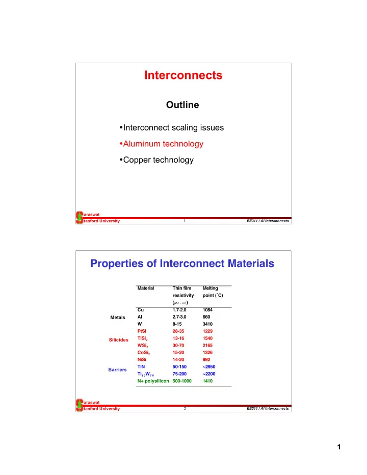
Interconnects Outline Interconnect scaling issues Aluminum technology Copper technology araswat tanford University EE311 / Al Interconnects 1 Properties of Interconnect Materials Material Thin film Melting resistivity point
Interconnects Outline • Interconnect scaling issues • Aluminum technology • Copper technology araswat tanford University EE311 / Al Interconnects 1 Properties of Interconnect Materials Material Thin film Melting resistivity point (˚C) ( µ � � cm ) Cu 1.7-2.0 1084 Metals Al 2.7-3.0 660 W 8-15 3410 PtSi 28-35 1229 TiSi 2 13-16 1540 Silicides WSi 2 30-70 2165 CoSi 2 15-20 1326 NiSi 14-20 992 TiN 50-150 ~2950 Barriers Ti 3 0 W 7 0 75-200 ~2200 N+ polysilicon 500-1000 1410 araswat tanford University EE311 / Al Interconnects 2 1
Interconnect Architecture SILICIDES - Short local interconnections which have to be exposed to high temperatures and oxidizing ambients, e.g., polycide and salicide structures. REFRACTORY METALS – Via plugs, future gate electrodes, local interconnections which need very high electromigration resistance. TiN, TiW – Barriers, glue layers, anti reflection coatings and short local interconnections. Al, Cu - for majority of the interconnects araswat tanford University EE311 / Al Interconnects 3 Why Aluminum? Al has been used widely in the past and is still used Low resistivity Ease of deposition, Dry etching Does not contaminate Si Ohmic contacts to Si but problem with shallow junctions Excellent adhesion to dielectrics Problems with Al • Electromigration ⇒ lower life time • Hillocks ⇒ shorts between levels • Higher resistivity araswat tanford University EE311 / Al Interconnects 4 2
Electromigration Electromigration induced hillocks and voids Electromigration due to electron wind induced diffusion of Al through grain boundaries void Metal Dielectric Void Hillock Metal SEM of hillock and voids formation due to electromigration in an Al line araswat tanford University EE311 / Al Interconnects 5 Electromigration Theory E field F TOTAL = F SCAT + F FIELD � qz � r F field + F scat E Where qz* is effective ion charge r r q � * Using Einstein’s relation � D = µ � kT � D � E = r r E J = � E = current density is related to E field by � Ea Diffusivity is given by D = D o e � kT � E a � D = J � qZ * kT Therefore kT D 0 e MTF � e Ea kT Meantime to failure is thus of the form of A � m Jn eEa kT γ is the duty factor A phenomenological model for MTF is MTF = M, n are constants araswat tanford University EE311 / Al Interconnects 6 3
Thermal Behavior in ICs 9 175 Maximum Power Dissipation 8 Chip Area [cm 2 ] 150 7 [W] 125 6 100 5 Source: ITRS 1999 4 75 50 70 90 110 130 150 170 190 Technology Node [nm] • Energy dissipated is increasing as performance improves • Average chip temperature is rising araswat tanford University EE311 / Al Interconnects 7 Parametric Dependencies of Electromigration Current Density Temperature r m J n exp E a A � � Mean time to failure is MTF = � � � kT � r is duty cycle J is current density E a is activation energy T is temperature A, m, and n are materials related constants araswat tanford University EE311 / Al Interconnects 8 4
Electromigration-Induced Integration Limits r m J n exp E a A � � MTF = � � r = duty cycle � kT � J =current density EM Limited Interconnect Width EM Limited Device Integration Density Ref: Yi, et al., IEEE Trans. Electron Dev., April 1995 Better packing techniques will be needed in the future to minimize the chip temperature rise araswat tanford University EE311 / Al Interconnects 9 Electromigration: Material and Composition Materials Composition Failure Time (hours) E a (eV) Cumulative failure (%) Temperature (K) Adding Cu to Al decreases its self Materials with higher activation diffusivity and thus increases energy have higher resistance to resistance to electromigration electromigration araswat tanford University EE311 / Al Interconnects 10 5
Electromigration: Grain Structure Top view Near bamboo structure Self Diffusion in Polycrystalline Materials D S D GB • For Al grain boundary diffusion D GB >> D s or D L (D s = surface diffusion, D L = lattice diffusion) • In a bamboo structure grain boundary diffusion is D L minimized araswat tanford University EE311 / Al Interconnects 11 Effect of Post Patterning Annealing on the Grain Structure of the Film. Increasing time Bamboo Structure and/or temperature With sufficient grain boundary migration a "bamboo structure" may develop No grain boundary diffusion in the bamboo structure araswat tanford University EE311 / Al Interconnects 12 6
Microstructural Inhomogeneities and Stress Induced Electromigration If the grain size is non uniform On an average the flux is uniform in the flux will vary accordingly. a uniform grain size textured film. electric current, J e- spanning grain A B atomic flux polygranular cluster cluster back flux from stress Polygranular cluster cluster � ss Tensile stress Compressive stress Spanning grain Spanning grain metal atom depletion metal atom accumulation tensile � (t 1 ) t o � o � (stress) t 1 build up of stress within polygranular t � comp. cluster with time due to electromigration L araswat tanford University EE311 / Al Interconnects 13 Build up of stress within polygranular cluster with time due to electromigration. � ss tensile � (t 1 ) t o � o � (stress) t 1 t � comp. L •Eventually, a steady-state is approached where the forward flux is equal to the backward flux due to stress. •A criterion for failure of an interconnect under electromigration conditions could be if the steady-state stress is equal to or greater than some critical stress for plastic deformation, encapsulent rupture, large void formation, etc. •The maximum steady state stress would occur at x=0 or x=L araswat tanford University EE311 / Al Interconnects 14 7
e- � ss � crit � crit � ss � � � ss � crit � ss � crit L 1 L 2 • For very large line width/grain size (w/d) values, no spanning grains are present. No points of flux divergence are present and the time to failure is relatively high. • As w/d decreases, some spanning grains occur. This results in divergences in the flux, causing stress to develop that can be greater than the critical stress for failure (with L > L crit for most or all of the polygranular clusters). The lines would fail and the median time to failure would decrease. • As w/d decreases more, more spanning grains are present, but the lengths of the polygranular cluster regions between them are shorter, many of them shorter than L crit . The stresses that develop, which create the back fluxes and which in turn eventually stop the electromigration flux, are in many cases smaller than the critical stress. • For small enough values of w/d bamboo or near-bamboo structures are present. The polygranular clusters are few, and for some lines, all the clusters are shorter than L crit and the lines will not fail by this mechanism. The MTTF thus increases dramatically. araswat tanford University EE311 / Al Interconnects 15 Electromigration: Grain Texture Empirical relationship (for Al & Al alloys) • MTF � e µ 2 log[ I (111) 3 ] S. Vaidya et al., Thin Solid Films, Vol. 75, 253, 1981 I (200) � 263 238 213 188°C 7 10 Time-to-Failure (sec) 6 10 (111) CVD Cu E a = 0.86 eV 5 10 (200) CVD Cu 4 10 E a = 0.81 eV 3 10 1.8 1.9 2.0 2.1 2.2 2.3 1/T (10 -3 /K) Ref: Ryu, Loke, Nogami and Wong, IEEE IRPS 1997. araswat tanford University EE311 / Al Interconnects 16 8
Layered Structures: Electromigration Layering with Ti reduces Electromigration e r Structure u l i a f Al-Si e v i t a l u m u Layered Al-Si/Ti C Time (arbitrary units) Improvements in layered films due to redundancy araswat tanford University EE311 / Al Interconnects 17 Mechanical properties of interconnect materials Material Thermal Elastic Hardness Melting expansion modulus, (kg/mm2) point coefficient (˚C) Y/(1- ) (MPa) (1/˚C) 23.1 x 10 -6 1.143 x 10 5 Al (111) 19-22 660 8.41 x 10 -6 1.699 x 10 5 Ti 81-143 1660 12.3 x 10 -6 TiAl 3 - 660-750 1340 2.6 x 10 -6 1.805 x 10 5 Si (100) - 1412 2.6 x 10 -6 2.290 x 10 5 Si (111) - 1412 0.55 x 10 -6 0.83 x 10 5 SiO 2 - ~1700 araswat tanford University EE311 / Al Interconnects 18 9
Layered Structures: Hillocks Pure Al Homogeneous Al/Ti Layered Al/Ti Surface profile Layering with Ti reduces hillock formation araswat tanford University EE311 / Al Interconnects 19 Stress due to Thermal Cycling Difference in the expansion coefficients of the film and substrate causes stress in the thin film. (a) Film as-deposited (stress free). (b) Expansion of the film and substrate with increasing temperature. (c) Biaxial forces compress the Al film to the substrate dimension araswat tanford University EE311 / Al Interconnects 20 10
Recommend
More recommend
Explore More Topics
Stay informed with curated content and fresh updates.
