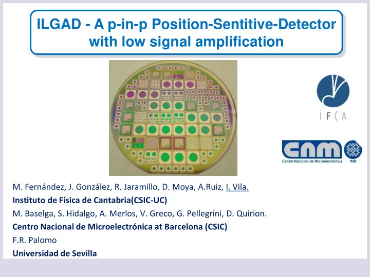
ILGAD - A p-in-p Position-Sentitive-Detector with low signal - PowerPoint PPT Presentation
ILGAD - A p-in-p Position-Sentitive-Detector with low signal amplification M. Fernndez, J. Gonzlez, R. Jaramillo, D. Moya, A.Ruiz, I. Vila. Instituto de Fsica de Cantabria(CSIC-UC) M. Baselga, S. Hidalgo, A. Merlos, V. Greco, G.
ILGAD - A p-in-p Position-Sentitive-Detector with low signal amplification M. Fernández, J. González, R. Jaramillo, D. Moya, A.Ruiz, I. Vila. Instituto de Física de Cantabria(CSIC-UC) M. Baselga, S. Hidalgo, A. Merlos, V. Greco, G. Pellegrini, D. Quirion. Centro Nacional de Microelectrónica at Barcelona (CSIC) F.R. Palomo Universidad de Sevilla
Work supported by RD50 - Radiation hard semiconductor devices for very high luminosity colliders. http://rd50.web.cern.ch/ RD50 participating Institutes in this project: CNM-Barcelona, G. Pellegrini, Giulio.Pellegrini@cnm-imb.csic.es Liverpool University, Gianluigi Casse, gcasse@hep.ph.liv.ac.uk UC Santa Cruz, Hartmut Sadrozinki, hartmut@ucsc.edu IFCA Santander, Ivan Vila, ivan.vila@csic.es University of Glasgow, Richard Bates, Richard.bates@glasgow.ac.uk INFN Florence, Mara Bruzzi, mara.bruzzi@unifi.it CERN, M. Moll, Michael.Moll@cern.ch Jozef Stefan Institute , G. Kramberger, Gregor.Kramberger@ijs.si IFAE Barcelona, S. Grinstein, sgrinstein@ifae.es INFN Torino, N. Cartiglia <cartiglia@to.infn.it> 2 I. Vila - ALCW 2015 April 20th, Tsukuba, Japan.
Outline — Motivations for the R&D. — Reach-through APD layout — Low Gain Avalanche Detectors: PADs and Microstrips. — Experimental characterization of LGADs — Inverse-LGAD: Layout and TCAD simulation. — Summary 3 I. Vila - ALCW 2015 April 20th, Tokio, Japan.
R&D Motivation — In a ILC environment with low hadron fluences and no active cooling, the material budget dominated by sensor’s material in the detector fiducial volume. — Implementing a small signal gain in microstrip sensors can reduce the thickness of the sensors without reducing the signal amplitude keeping the same SNR ratio. — A relatively small signal gain (5-10) needed to allow the use of standard readout front-end without signal saturation. 4 I. Vila - ALCW 2015 April 20th, Tokio, Japan.
Enabling technology: Reach-Trough Avalanche Photo-Diodes (1) — RT-APD , lightly doped p-substrate with two- diffusions to created a local high-field region (impact ionization signal multiplication) — Low Gain Avalanche Detector ( LGAD ): the gain p- layer engineered (doping and depth) to achieve low signal gain. 5 I. Vila - ALCW 2015 April 20th, Tokio, Japan.
LGADs: Technical challenges Electric Field @ 400 V N + P π Core Region Uniform electric field, high enough to activate mechanism of impact ionization (multiplication) Termination High electric field confined in the core region 𝑾 𝑪𝑬 | 𝐔𝐟𝐬𝐧𝐣𝐨𝐛𝐮𝐣𝐩𝐨 ≫ 𝑾 𝑪𝑬 | 𝑫𝒇𝒐𝒖𝒔𝒃𝒎 Periphery (Dead region) Charges should not be collected. Reduction of the leakage currents 6 I. Vila - ALCW 2015 April 20th, Tokio, Japan.
PAD LGAD: Gain and Noise G. Kramberger — Small noise excess factor (introduced by the stochastic nature of the multiplication process. 7 I. Vila - ALCW 2015 April 20th, Tokio, Japan.
PAD LGAD: Red laser TCT characterization Electron multiplication h+ drift e-h pairs 285 um generation e- drift Bottom injection Red laser (670 nm) I (Arb. Unit) STANDARD PIN DIODE LGAD DIODE 5ns Current from Current from Current from primary electrons secondary holes primary electrons Time 8 I. Vila - ALCW 2015 April 20th, Tokio, Japan.
PAD LGAD : Response uniformity. 9 I. Vila - ALCW 2015 April 20th, Tokio, Japan.
Strip LGAD: Segmented applification N on P microStrips. PiN vs LGAD Aluminum Passivation N+ Cathode P-Stop P-Multiplication 10 I. Vila - ALCW 2015 April 20th, Tokio, Japan.
Strip LGAD: Amplification region geometry — Several layouts with different p-well width and n-well depth were manufactured. — BUT most of them presented reduced breakdown voltage and large inverse current. A new run with optimized p-well engineering just produced. — A few samples displayed breakdown voltage above depletion voltage. There were tested with microspot ion beams and x-rays. 11 I. Vila - ALCW 2015 April 20th, Tokio, Japan.
Strip LGADs: Ion Beam Induced Charge (1) — Ion Beam Induced Charge at Centro Nacional de Aceleradores in Seville. 12 I. Vila - ALCW 2015 April 20th, Tokio, Japan.
Strip LGAD: Ion Beam Induced Charge(2) 13 I. Vila - ALCW 2015 April 20th, Tokio, Japan.
Strip LGAD: Ion Beam Induced Charge (3) 14 I. Vila - ALCW 2015 April 20th, Tokio, Japan.
Strip LGAD: X-Ray (Diamond Light Source) R. Bates D. Maneuski 15 I. Vila - ALCW 2015 April 20th, Tokio, Japan.
Strip LGAG: New run available — Improved amplification p-well engineering. 16 I. Vila - ALCW 2015 April 20th, Tokio, Japan.
p-in-p Strip LGAD:The “Inverse” LGAG — Double-sided LGAD with pad-like multiplication structure in the back-side and ohmic read out strips in the front side N on P vs P on P LGAD microStrips Comparison 17 I. Vila - ALCW 2015 April 20th, Tokio, Japan.
ILGAD: Pad diode with segmented back-side N + Cathode P-type multiplication layer JTE P-type ( π )substrate P Stop P + Anode 18 I. Vila - ALCW 2015 April 20th, Tokio, Japan.
ILGAD – TCAD Validation (1) 2D simulation of three p-on-p microstrip LGAD Electric Field 2D Distribution. Maxim @ Junctions STRIP I-LGAD STRIP LGAD 19 I. Vila - ALCW 2015 April 20th, Tokio, Japan.
ILGAD – TCAD Validation (2) MIP through the middle of the sensors (the central strip) @ 100 V 50 um thick substrate ILGAD STANDARD 20 I. Vila - ALCW 2015 April 20th, Tokio, Japan.
Summary — Strip sensors with moderated signal gain could significantly reduce the tracking material budget. — Low gain Reach-Through APD architecture successfully implemented and tested in “pad” detectors ( LGAD ) — LGAD implemented in n-in-p microstrips sensors with segmented amplification region (anode). — No gain observed so far in strips LGAD, new batch with optimized amplification p-well. — New design of double-sided p-in-p microstrip LGADs with cathode strip-like segmented cathode as readout ( ILGAD ) — ILGAD TCAD Validation uniform amplification region and V BD in main junction. 21 I. Vila - ALCW 2015 April 20th, Tokio, Japan.
どうもありがとう ございます Doumo arigatou gozaimasu 22 I. Vila - ALCW 2015 April 20th, Tokio, Japan.
Recommend
More recommend
Explore More Topics
Stay informed with curated content and fresh updates.

