Happy birthday PL Imaging! SPREE Seminar 15 December 2016 Contents - PowerPoint PPT Presentation
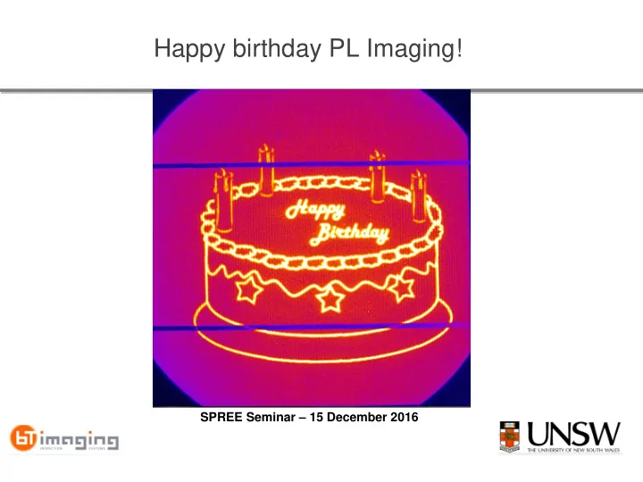
Happy birthday PL Imaging! SPREE Seminar 15 December 2016 Contents The importance of good upbringing Born in AUS, a healthy baby! Baby step, finding your place in the world. Now an adolescent, knowing it all. -
Happy birthday PL Imaging! SPREE Seminar – 15 December 2016
Contents • The importance of good upbringing… • Born in AUS, a healthy baby! • Baby step, finding your place in the world. • Now an adolescent, “knowing it all…”. - but yet a lot to learn!
The importance of “good upbringing”. Universität Karlsruhe, Germany Prof Peter Würfel • Lifetime achievements in the “Physics of Solar cells”. • Early adopter, recognizing the potential of luminescence. • “Grandfather” of PL imaging!
Some background • The generalised Planck equation: 2 2 n 1 dr , T , T d sp BB 2 3 2 c X 0 exp 1 kT Emission spectrum is determined by the absorption properties. Emission intensity is determined by the separation of the quasi Fermi energies. W. van Roosbroeck and W. Shockley, Phys.Rev. 94, 1558 (1954). P. Würfel, J. Phys. C 15, 3967 (1982).
Some background I lum ~ exp ~ exp kT kT Quantitative information about from PL intensity! Implied voltage measurements. 2 I ~ n p n ( n N ) n exp lum A / D i kT Quantitative information about n from PL intensity! QSS-PL minority carrier lifetime measurements.
Early days… First QSS-PL data presented in 2004 T. Trupke, R.A. Bardos, F. Hudert, P. Würfel, J. Zhao, A. Wang, M.A. Green, 19th European Photovoltaic Solar Energy Conference, Paris, France, June 2004. • LED based QSS-PL >100ms on 1000 W cm n-type wafer • • Data controversial (we will see!) • Ron seemed to like it…
2004: QSS-PL lifetime 70 60 Effective Lifetime / s • 50 Excellent agreement PL between QSS-PL and 40 PC QSS-PC 30 20 10 1E12 1E13 1E14 -3 Excess Carrier Concentration n / cm
2004: QSS-PL lifetime 500 • QSS-PL immune to PC Apparent Lifetime / s 400 trapping. • Calibration not trivial. 300 PC with sub band • QSS-PC still most widely 50W gap illumination 200 used today. 250W • Complementary 100 techniques. PL 0 10 11 12 13 14 15 10 10 10 10 10 10 -3 Excess Carrier Concentration / cm
2004 – PL mapping • Scanning spectral PL tool, 50mm x 50mm, micron resolution. • Slow “Let’s try camera based PL imaging!”
May 2005 – Can we actually afford this? A weekend email makes all the difference “Hi Martin, Rob and I plan to expand our experimental work on QSS-PL to PL imaging. We would need ~ $ 50,000 to set up a proof of concept system. TT” “Hi Thorsten, that sounds promising, I am happy to support characterisation work at UNSW, pls get the account number from Jenny on Monday. More funding available for this if required. MAG”
Making it happen - quickly! Mid 2005 : First PL imaging prototype in EE building, LG 24 . • The 100W laser challenge… • The mapping tool had to go… • First PL image, a Eureka moment! • Huge Excitement for months. • System is still in operation at UNSW.
First PL images • • Up to several hrs 1s <100 m per pixel • • Typically 1mm per pixel
Baby steps – learning to walk 2005 : Qualitative PL imaging • Wide range of material- and process induced faults detectable • Rapid adoption by the UNSW high efficiency group and the buried contact solar cell group for routine daily process monitoring
Baby steps – learning to walk 2006 : Calibrated minority carrier lifetime images Carrier Density Image (CDI) PL imaging • Calibration via QSS-PC best option T. Trupke, R.A. Bardos, M.C. Schubert and W. Warta , Photoluminescence imaging of silicon wafers , Appl.Phys.Lett. 89 , 044107 (2006).
First paper – official birthday! The first PL image Rob Thorsten 26 Jul 2006 9.00am 1 Mpixel 1s (Resolution) (Acquisition time) LG24 UNSW Australia
Baby steps – learning to walk 2006: c-Si workshop, Denver EL image PL image PL image with current extraction • Proposal to use PL for R s imaging • But why does thi s happen…?
Baby steps – learning to walk Why do Rs variations within a cell show up in luminescence images? R S I lum exp exp kT kT • J 0 EL: High Rs causes lower junction J 0 + voltage Low PL intensity - • PL: No current flow, no impact of Rs on junction voltage. • PL SC : High Rs impedes local current extraction High relative PL intensity
Baby steps – learning to walk 2007: Quantitative Rs imaging • Rs imaging based on at least two images: • Voc • MPP • Good separation of R s from lifetime Quantitative effective local R s in W cm 2 • • Several PL/EL based R S methods followed • “PL emission at zero voltage! What the heck …?” “Voltage independent carriers” T. Trupke, E. Pink, R. A. Bardos, and M. D. Abbott. Appl.Phys.Lett. 90 , 093508 (2007). H. Kampwerth, T. Trupke, J. Weber, Y. Augarten, Appl.Phys.Lett. 93 . 202102 (2008).
Baby steps – learning to walk 2016: Voltage independent carriers • Presence of voltage independent carriers follows from the continuity equation: • Voltage dependent term: • Voltage independent term: Mattias Juhl, manuscript submittted
Baby steps – learning to walk 2016: Voltage independent carriers Applied voltage in the dark Illumination with l exc =1100nm Illumination with l exc =1100nm, external SC Excess carrier profile under illumination at SC is present at all bias conditions First order correction by subtracting PLsc from PL at other bias conditions. Poster by Mattias Juhl at this workshop!
Growing up Finding your place in the world From 2007: • PL imaging activities at UNSW, ANU, ISE, ISFH, NREL, Uni Konstanz, MPI, ISAS/JAXA… • Lifetime imaging and dynamic calibration methods • Series resistance imaging • Diffusion length imaging on cells • J 0 , J 0e imaging • J sc imaging • Efficiency imaging • Shunt detection and quantification • Bulk lifetime imaging on bricks • Fe (and other atomic defects) concentration imaging • High throughput as-cut wafer imaging • …
Growing up Finding your place in the world Late 2007: • Interest in PL imaging systems from industry after 2006 presentations (e.g. WCPEC 2006) • BT imaging founded • Jørgen Nyhus from REC, first adopter (UNSW visit in Dec 2007, First PO for R1)! • LIS-R1 presented at 2008 EUPVSC, Milan. • Commercially availability PL imaging systems enable rapid adoption throughout PV industry.
Growing up Finding your place in the world 2011: Line scanning PL imaging Area scanning Line scanning • Line illumination • Measurement on the fly, e.g. 300mm/s
Growing up Finding your place in the world 2011: Line scanning PL imaging Area scanning Line scanning • Line illumination • Measurement on the fly, e.g. 300mm/s
Growing up Finding your place in the world As cut wafer inspection • Metrics can be extracted from PL images using automatic image processing. Impure edges Dislocations
Growing up Finding your place in the world As cut wafer inspection
Growing up Finding your place in the world As cut wafer inspection • PL imaging used today for IQC/OQC in production at up to 5,400 wph. • Correlation of cell efficiency defect density with PL metrics • Not detectable with sufficient throughput with any other technique.
Growing up Finding your place in the world 2009: Brick inspection Brick d=200 m Wafer Effective lifetime eff Bulk lifetime dependence strongly non-linear. Virtually no variation for t b > 10 s. • 0.1 1 10 100 1000 Bulk Lifetime / s
Growing up Finding your place in the world 2007: PL Intensity ratio (PLIR) method Emission spectrum changes depending on the depth from the surface! P. Würfel, T. Trupke, T. Puzzer, E. Schäffer, W. Warta, S.W. Glunz, Diffusion Lengths of Silicon Solar Cells from Luminescence Images , J.Appl.Phys. 101 , 123110 (2007).
Growing up Finding your place in the world 2009: Brick inspection • PL imaging on bricks • How to quantify? I ~ n p n N N lum D / A eff D / A
Growing up Finding your place in the world 2011: Bulk lifetime imaging from PLIR 1 st PL image measured with a SP filter 2 nd PL image measured with a LP filter I PL, SP PLIR= I PL, LP • Absolute lifetime from first principles. • Background doping cancels in PLIR! B. Mitchell, T. Trupke, J. W. Weber, and J. Nyhus, J. Appl. Phys. 109 , 083111 (2011).
Growing up Finding your place in the world 2011: Bulk lifetime imaging from PLIR p-type multi: n-type Cz: 0.2 s < b Measured b up to 7 ms Background doping variations cancel out in PLIR Bulk lifetime as quality specification for wafers Cutting guide
Bulk lifetime on bricks and thick wafers 2015 2011 Structural defect analysis D. Chung, B. Mitchell, J.W. Weber and T. Trupke, MRS Spring meeting 2016, Phoenix, USA, March 2016
Bulk lifetime on bricks and thick wafers Automatic defect analysis
Recommend
More recommend
Explore More Topics
Stay informed with curated content and fresh updates.
