from atoms to systems www.tyndall.ie Nanotechnology Designed for - PowerPoint PPT Presentation
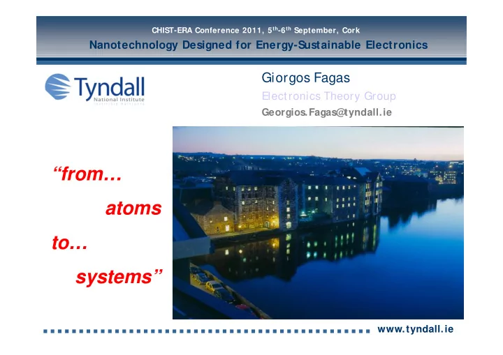
CHIST-ERA Conference 2011, 5 th -6 th September, Cork Nanotechnology Designed for Energy-Sustainable Electronics Giorgos Fagas Electronics Theory Group Georgios.Fagas@tyndall.ie from atoms to systems www.tyndall.ie
CHIST-ERA Conference 2011, 5 th -6 th September, Cork Nanotechnology Designed for Energy-Sustainable Electronics Giorgos Fagas Electronics Theory Group Georgios.Fagas@tyndall.ie “from… atoms to… systems” www.tyndall.ie
Nanotechnology Designed for Energy-Sustainable Electronics Agenda the Grand challenge (or… why are we here? ) Energy consumption on the rise Consumer electronics opportunities for ICT (or… what can we do? ) Low-power (autonomous) devices (More-Moore) Devices for energy efficiency (More-than-Moore) a nano-inspired bottom-up approach (or… why nanotechnology? ) From atoms to materials to devices more Moore: ideal sub-threshold slopes at the nanoscale more than Moore: nanomaterials for energy harvesting expected impact (or… what are the outputs?) www.tyndall.ie www.tyndall.ie
Nanotechnology Designed for Energy-Sustainable Electronics the Grand challenge opportunities for ICT a nano-inspired bottom-up approach expected impact www.tyndall.ie
ICT energy pie grows fast! ICT and consumer electronics account for approximately 15% of global residential electricity consumption Data: IEA report (2009) www.tyndall.ie www.tyndall.ie
1,700 TWh in two decades! By 2030, energy use by household ICT and consumer electronics will triple consuming 1,700TWh 4,344 TWh 3,457 TWh 1,038 TWh Maps: http://en.wikipedia.org Data: IEA report (2010) www.tyndall.ie www.tyndall.ie
Nanotechnology Designed for Energy-Sustainable Electronics the Grand challenge opportunities for ICT a nano-inspired bottom-up approach Co-design of nanotechnology-enhanced ICT expected impact www.tyndall.ie
Technology Booster 1 Elements used in Chip Fabrication Courtesy J.-P. Colinge www.tyndall.ie www.tyndall.ie
Technology Booster 2 Mobility enhancement by strain pMOS: compressive strain nMOS: tensile strain A 90nm High Volume Manufacturing Logic Technology Featuring Novel 45nm Gate Length Strained Silicon CMOS Transistors T. Ghani et al, IEDM 2003, p. 978 www.tyndall.ie www.tyndall.ie
Technology Booster 3 Evolution of Transistors Geometry “Gate-all-Around” “Gate-all-Around” Courtesy J.-P. Colinge “3 Gates” “3 Gates” “2 Gates” “2 Gates” Source Gate “1 Gate” “1 Gate” Drain I D Polysilicon Gate Buried oxide Gate Silicon Source Drain Fin – Gate – Gate BOX Buried Oxide 20 nm Gate Source Drain Buried oxide Back gate (substrate) www.tyndall.ie www.tyndall.ie
Transistor scaling why nanowires? R. S. Chau, Technology@Intel Magazine (2006) Intel 22nm Ivy Bridge (2011) www.tyndall.ie www.tyndall.ie
Semiconducting Nanowire Platform for Autonomous Sensors SiNAPS SiNAPS mote concept (see www.sinaps-fet.eu) Si NW modified Ge Energy Scavengers CMOS module NW modified CMOS module Micro-fluidics Integrated Sensors CMOS module Logics and Transmittance I O www.tyndall.ie www.tyndall.ie
Nanoelectronics meets atomic design Top-down Sing et al , IEEE TED 55 , 3107 (2008) Bottom-up Ma et al , Science 299 , 1876 (2003) size convergence with atomic-scale modelling www.tyndall.ie www.tyndall.ie
TCAD tools hierarchy R.W. Dutton and A.J Strojwas, IEEE Trans. CAD of ICS 19, 1544 (2000) www.tyndall.ie www.tyndall.ie
Co-design of nanotechnology-enhanced ICT a-priori technology evaluation and design Energy Micro/Nano Photonics harvesting electronics Design for manufacturing, circuit models TCAD Device New designs, architectures, and materials modelling Materials IV & III-V nanomaterials, alloys, functional oxides research Atomic-scale fundamentals www.tyndall.ie www.tyndall.ie
Nanotechnology Designed for Energy-Sustainable Electronics the Grand challenge opportunities for ICT a nano-inspired bottom-up approach Example 1: ideal sub-threshold slopes at the nanoscale expected impact www.tyndall.ie
Junctionless transistor Gated Resistor (or CMOS without junctions) no doping gradients The cross-section of the channel is small enough that gate can deplete the heavily doped channel (8 x 10 19 cm -3 ) entirely, hence can turn off device x x J-.P. Colinge et al, Nat. Nanotech. 5 , 225 (2010) www.tyndall.ie www.tyndall.ie
Junctionless transistor characteristics dV G SS d log I D J-.P. Colinge et al, Nat. Nanotech. 5 , 225 (2010) x x new devices show even smaller short channel effects www.tyndall.ie www.tyndall.ie
Dopant profile issue L L? “Ultrashort channel” “Short channel” (<10nm) (35nm) “Junctionless” “Junctionless” www.tyndall.ie www.tyndall.ie
Dopants in nanowires fundamental limitation for junctions Mulliken population analysis Δ Q = Q n-type - Q intrinsic at Vg = 0 V Position of doping atoms wire axis (Å) localization radius of the dopant electron or hole is ~ 1.5 nm L. Ansari, B. Feldman, G. Fagas, J-.P. Colinge, and J. C. Greer, Appl. Phys. Lett. 97 , 062105 (2010) www.tyndall.ie www.tyndall.ie
(Junctionless) transistor scaling Classical device simulation C.W. Lee et al , Appl. Phys. Lett. 94 , 053511 (2009) Gate length L g > 10nm Experimental device J-.P. Colinge et al , Nature Nanotech. 5 , 225 (2010) Geometry dependence in classical and quantum devices P. Razavi et al , submitted (2011) Using realistic electronic structure, can the device scale down to sub-5nm? x x www.tyndall.ie www.tyndall.ie
Transistor behaviour at 3nm p-type (Ga doped) 8 x 10 20 cm -3 L. Ansari, B. Feldman, G. Fagas, J-.P. Colinge, and J. C. Greer, Appl. Phys. Lett. 97 , 062105 (2010) www.tyndall.ie www.tyndall.ie
Subthreshold slope ~ 80 mV /decade near to theoretical limit! L. Ansari, B. Feldman, G. Fagas, J-.P. Colinge, and J. C. Greer, Sol. Stat. Elec. (2011) www.tyndall.ie www.tyndall.ie
Si and CNT JL transistors comparison – 5.4 nm L. Ansari et al, in preparation www.tyndall.ie www.tyndall.ie
Nanotechnology Designed for Energy-Sustainable Electronics the Grand challenge opportunities for ICT a nano-inspired bottom-up approach Example 2: nanomaterials for energy harvesting expected impact www.tyndall.ie
Energy harvesting possibilities Battery operated systems R. J. M. Vullers, Zero-Power ICT Workshop 2009 Ambient energy R. J. M. Vullers et al , Solid-State Elec. 53 , 684 (2009) www.tyndall.ie www.tyndall.ie
Axial junctions in nanowire arrays p + n + n antireflection effect in NW arrays up to 4.4% efficiency under 1-sun illumination http://en.wikipedia.org V. Sivakov, G. Andrä, A. Gawlik, A. Berger, J. Plentz, F. Falk, S.H. Christiansen, Nano Lett. 9 , 1549 (2009) www.tyndall.ie www.tyndall.ie
Arrays of nanowire coaxial cables a b 80 AM 1.5 2 Contact area: 7.02 mm 2 ) 70 Dark Current density (mA/cm Efficiency: 7.29% 500nm 500nm 60 Open circuit voltage: 476 mV 2 50 Current density: 27.03 mA/cm c d Filling factor: 0.562 40 30 20 500nm 500nm 10 0 -10 -20 -30 -1,2 -1,0 -0,8 -0,6 -0,4 -0,2 0,0 0,2 0,4 0,6 0,8 1,0 Voltage (V) Guobin Jia, Martin Steglich, Ingo Sill, and Fritz Falk (IPHT), 2011 www.tyndall.ie www.tyndall.ie
Towards miniaturisation robust performance against thin film solar cells PV technology platform sets poly- Si thickness <100µm in 2030 Efficiency: 4.83% 20µm thick Si absorber 8µm thick Si absorber Erik Garnett and Peidong Yang, Nano Lett. 10 , 1082 (2010) www.tyndall.ie www.tyndall.ie
Atomic structure of a-Si (a-Si:H) heat and quench MD method for structure generation K. Laaziri et al, PRB 60, 13520 (1999) a-Si cell of 512 atoms melt at 3500K – quench at 300K radial distribution function M. Legesse, M. Nolan and G. Fagas, unpublished www.tyndall.ie www.tyndall.ie
Electronic properties of hydrogenated a-Si experiment first-principles D.V. Lang et al, PRB 25, 5285 (1982) log of DOS vs energy (eV) for aSi:H (12%H) M. Legesse, M. Nolan and G. Fagas, unpublished www.tyndall.ie www.tyndall.ie
New materials for transparent electronics CRYSTAL STRUCTURE OF Ba-doped SrCu 2 O 2 ; Challenge: A p-type transparent blue=Ba, green=Sr, pink=Cu, red=O. conducting oxide (TCO) for transparent electronics. Question Posed: Can we use modelling to design a new p-type TCO instead of traditional trial- and-error approach? Results: Predicted a novel TCO, with optimal composition for Ba distorts the structure, reducing Cu-Cu transparency: Ba-doped SrCu 2 O 2 . interactions and increasing the transparency to visible light. By contrast, other dopants reduce the transparency. Experiments by European SrCu 2 O 2 Ba-doped partners confirmed its properties. SrCu 2 O 2 doping widens band gap more transparent to Material was licensed to Umicore visible light and patented. M. Nolan & S. D. Elliott, Chem. Mater. 20, 5522 (2008) SCHEMATIC ELECTRONIC STRUCTURE showing gap between conduction band and Cu-derived valence band www.tyndall.ie www.tyndall.ie
Nanotechnology Designed for Energy-Sustainable Electronics the Grand challenge opportunities for ICT a nano-inspired bottom-up approach expected impact www.tyndall.ie www.tyndall.ie
A modelling hierarchy for nano-inspired bottom-up technology design • Customer Need • Process S imulation • Device Modelling • Parameter Extraction • Compact Models • Circuit S imulation 30%-40% cost reduction www.tyndall.ie www.tyndall.ie
Recommend
More recommend
Explore More Topics
Stay informed with curated content and fresh updates.
