ECE321 Electronics I Fall 2006 Professor James E. Morris Lecture 3 - PDF document
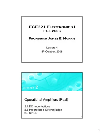
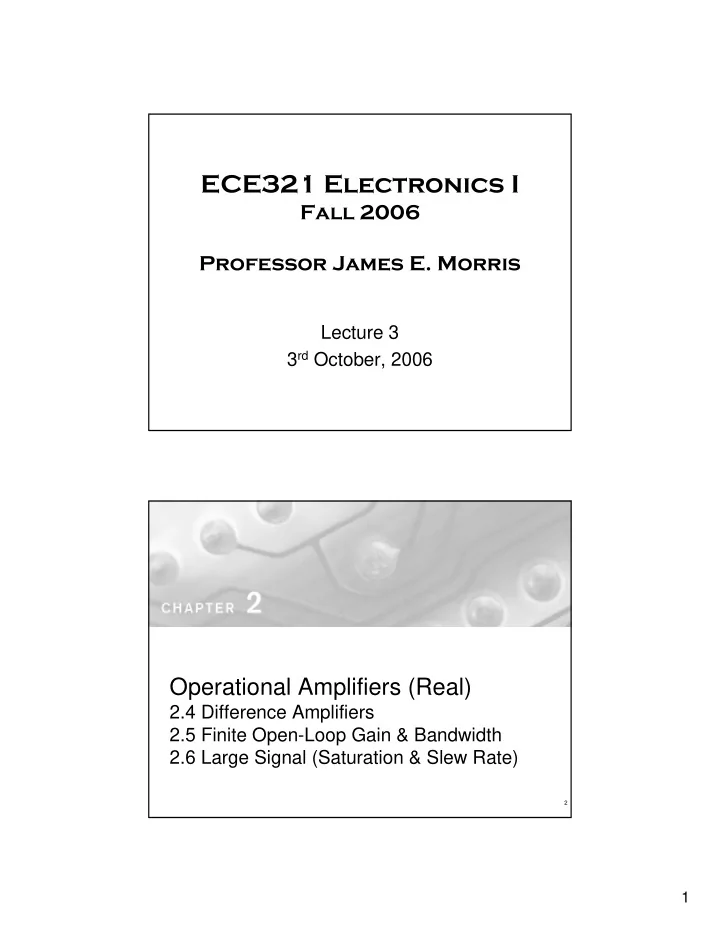
ECE321 Electronics I Fall 2006 Professor James E. Morris Lecture 3 3 rd October, 2006 Operational Amplifiers (Real) 2.4 Difference Amplifiers 2.5 Finite Open-Loop Gain & Bandwidth 2.6 Large Signal (Saturation & Slew Rate) 2 1 Figure
ECE321 Electronics I Fall 2006 Professor James E. Morris Lecture 3 3 rd October, 2006 Operational Amplifiers (Real) 2.4 Difference Amplifiers 2.5 Finite Open-Loop Gain & Bandwidth 2.6 Large Signal (Saturation & Slew Rate) 2 1
Figure 2.15 Representing the input signals to a differential amplifier in terms of their differential and common-mode components. Figure 2.16 A difference amplifier. 2
Figure 2.17 Application of superposition to the analysis of the circuit of Fig. 2.16. Figure 2.18 Analysis of the difference amplifier to determine its common-mode gain A cm ; v O / v Icm . 3
Figure 2.19 Finding the input resistance of the difference amplifier for the case R 3 = R 1 and R 4 = R 2 . Figure 2.20 A popular circuit for an instrumentation amplifier: (a) Initial approach to the circuit; (b) The circuit in ( a ) with the connection between node X and ground removed and the two resistors R 1 and R 1 lumped together. This simple wiring change dramatically improves performance; (c) Analysis of the circuit in‘ (b) assuming ideal op amps. 4
Figure 2.20 A popular circuit for an instrumentation amplifier: (a) Initial approach to the circuit; (b) The circuit in ( a ) with the connection between node X and ground removed and the two resistors R 1 and R 1 lumped together. This simple wiring change dramatically improves performance; (c) Analysis of the circuit in‘ (b) assuming ideal op amps. Figure 2.21 To make the gain of the circuit in Fig. 2.20(b) variable, 2 R 1 is implemented as the series combination of a fixed resistor R 1 f and a variable resistor R 1 v . Resistor R 1 f ensures that the maximum available gain is limited. 5
Figure 2.22 Open-loop gain of a typical general-purpose internally compensated op amp. Figure 2.23 Frequency response of an amplifier with a nominal gain of +10 V/V. 6
Figure 2.24 Frequency response of an amplifier with a nominal gain of –10 V/V. Figure 2.25 (a) A noninverting amplifier with a nominal gain of 10 V/V designed using an op amp that saturates at ± 13-V output voltage and has ± 20-mA output current limits. (b) When the input sine wave has a peak of 1.5 V, the output is clipped off at ± 13 V. 7
Figure 2.26 (a) Unity-gain follower. (b) Input step waveform. (c) Linearly rising output waveform obtained when the amplifier is slew-rate limited. (d) Exponentially rising output waveform obtained when V is sufficiently small so that the initial slope ( v t V ) is smaller than or equal to SR. Figure 2.27 Effect of slew-rate limiting on output sinusoidal waveforms. 8
Recommend
More recommend
Explore More Topics
Stay informed with curated content and fresh updates.


