Design of Dottorando Ing.Davide Microwave Absorbing Structure - PowerPoint PPT Presentation
Sapienza Universit di Roma Scuola di Ingegneria Aerospaziale DOTTORATO DI RICERCA XXIII CICLO Tesi di Dottorato Design of Dottorando Ing.Davide Microwave Absorbing Structure Micheli and Microwave Shielding Structure Tutor By using
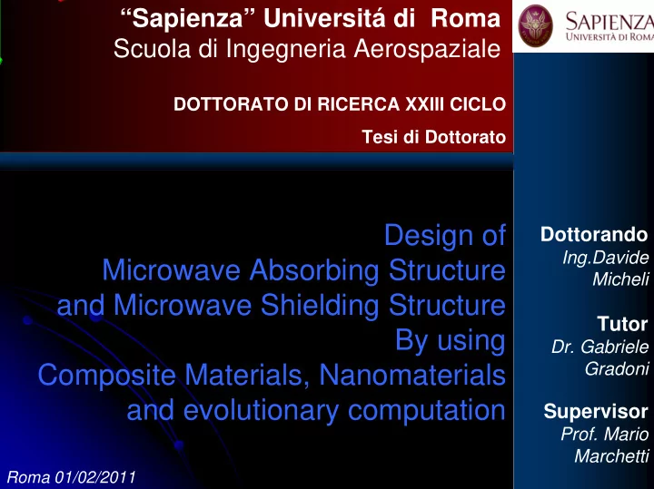
“Sapienza” Universitá di Roma Scuola di Ingegneria Aerospaziale DOTTORATO DI RICERCA XXIII CICLO Tesi di Dottorato Design of Dottorando Ing.Davide Microwave Absorbing Structure Micheli and Microwave Shielding Structure Tutor By using Dr. Gabriele Gradoni Composite Materials, Nanomaterials and evolutionary computation Supervisor Prof. Mario Marchetti 1 1 Roma 01/02/2011
Topics Topics EMI: shielding and absorbing 1 Target: Modeling microwave 2 5 Absorbing Material using Electromagnetic Experimental validation carbon nano-materials absorbing model of absorber model end 5 Evolutionary 4 3 computation 2 1 0 3 4 -1 -2 -3 -4 -5 -5 -4 -3 -2 -1 0 1 2 3 4 5 Carbon Nano-materials and Absorber design 2 2 dielectric characterization Evolutionary computation modeling
Topics Topics EMI: shielding and absorbing 1 Target: Modeling microwave 2 5 Absorbing Material using Electromagnetic Experimental validation carbon nano-materials absorbing model of absorber model end 5 Evolutionary 4 3 computation 2 1 0 3 4 -1 -2 -3 -4 -5 -5 -4 -3 -2 -1 0 1 2 3 4 5 Carbon Nano-materials and Absorber design 3 3 dielectric characterization Evolutionary computation modeling
Why EMI Shielding and Absorbing ? Why EMI Shielding and Absorbing ? EMI de finitio n Electromagnetic Interference (EMI), defined by NATO as an electromagnetic disturbance which interrupts, obstructs, or otherwise degrades the effective performance of electronic or electrical equipment.( www.glenair.com/html/emi.htm). SISTEMS AFFECTED AND GENERATING EM DISTURBNCES PC EM shield Cellular Phone Satellites War scenario Anechoic Chamber Stealthness Electronic war Lightning Radar TLC system
Why EMI Shielding and Absorbing ? Why EMI Shielding and Absorbing ? NASA Contractor Report 4784 Design Guidelines for Shielding Effectiveness, Current Carrying Capability, and the Enhancement of Conductivity of Composite Materials •Electromagentic compatibility (EMC) occurs when all equipment in a system operates properly without electronic interference from equipment within or outside the system. •Electromagentic interference (EMI) occurs when there is a source of emission and a unit that is susceptible and a mtehod of tranmsission between the two. •Such interference can be controlled reducing unnecessary emission, susceptibility, and/or interrupting the transmission path.
Why EMI Shielding and Absorbing ? Why EMI Shielding and Absorbing ? NASA Reference Publication 1374. In time period up to 1993 N° 17 Case histories of spacecraft, and N° 120 Case histories military and civil apparatus failure or anomalies attributed to EMI Some NASA cases histories: A low level signal not always present and not due spurious of radio station or mobile transmitters, interfere with on board Saturn V vehicle sub-system. Investigation revealed that Carbon-arch- lamps surrounding the vehicle, were producing broadband frequency disturbances. During checkout of Skylab Apollo Telescope, an EMC test illuminated the entire Skylab with various transmitter frequencies. This revealed failure in the Telemetry system.
Why EMI Shielding and Absorbing ? Why EMI Shielding and Absorbing ? Some Non NASA cases histories Disasters caused by EMI problems In 1967 in Vietnam, a Neavy jet landing experienced an uncommanded release of munitions that struck a fully armed and fueled fighter on deck. The results were explosion, the dead of 134 sailors. This accident was caused by the Radar illuminating the landing aircraft. The resulting EMI sent an unwanted signal to the weapons system. During the early years of ABS’s, Mercedes automobiles equipped with ABS had severe braking problems along a certain stretch of German autobahn. The brakes where affected by a near-by radio transmitter as drivers applied them on the curved section of highway. The nearterm solution was to erect a mesh screen along the roadway to attenuate the EMI.
Why EMI Shielding and Absorbing ? Why EMI Shielding and Absorbing ? Stealthness Military applications
Topics Topics EMI: shielding and absorbing 1 Target: Modeling microwave 2 5 Absorbing Material using Electromagnetic Experimental validation carbon nano-materials absorbing model of absorber model end 5 Evolutionary 4 3 computation 2 1 0 3 4 -1 -2 -3 -4 -5 -5 -4 -3 -2 -1 0 1 2 3 4 5 Carbon Nano-materials and Absorber design 9 9 dielectric characterization Evolutionary computation modeling
Electromagnetic absorbing theory Electromagnetic absorbing theory PRINC IPL ES O F ABSO RBER O PERAT IO N When a certain interface separating different material is encountered, incoming electromagnetic waves are in part reflected and in part transmitted through material. EM Transmission attenuation (dB), determines the EM Shielding properties of Materials or Structure EM Interference wave Transmitted Interference wave EM Reflected components determines the amounts in interference presence Lossy material
Electromagnetic absorbing theory Electromagnetic absorbing theory PRINC IPL ES O F ABSO RBER O PERAT IO N From Maxwell equation such system can be well studied using the equivalent transmission line equations and schemes l 2 η 1 η 2 η 3 Incoming wave Transmitted wave • Since the material wave impedance η is Reflected different from free space impedance η wave there will be impedance mismatch and this will create the reflected wave. η − η Lossy Γ = 1 2 η + η material • Since the material will always have 1 2 some losses, there will be attenuation η 1 η 2 η 3 of the incident power
Absorbing Structure Absorbing Structure Layers are characterized by different values of ε k giving the k th -layer transverse characteristic impedances TM and TE upon electromagnetic wave incidence angle θ k µ µ η = ϑ TM 0 rk cos k ε ε k 0 rk µ µ 1 η = TE 0 rk k ε ε ϑ cos 0 rk k ⎛ ⎞ ε ⎜ ⎟ + 1 sin r ϑ = k ϑ arcsin ⎜ + ⎟ k k 1 ε ⎝ ⎠ r k where for Snel’s law
Absorbing Structure Absorbing Structure In Absorbing applications, RC at the air-absorber interface can be evaluated by the following equation relating the free space impedance to the input impedance seen at the air-multilayer structure interface where Z 0 ≅ 377 Ω is the free space impedance and Z i is the input − TM / TE TM / TE Z Z impedance at the first air-absorber = TM / TE 1 i 0 RC interface. The input wave impedance of + / / TM TE TM TE Z Z the multilayer, backed by PEC, can be i 0 expressed iterating the following equation for each layer k ( ) ( ) t k is the layer k β + η β TM / TE TM / TE Z cos t j sin t = η − thickness in m , TM / TE TM / TE ik 1 k k k k k Z ( ) ( ) 2 η β + β ik k TM / TE TM / TE whereas the cos t jZ sin t − k k k ik 1 k k wave number is β k ( ) β = π µ ε µ ε ϑ = π µ ε µ ε − ε ϑ 3 2 f cos 2 f ' j " cos k 0 0 rk rk ik 0 0 rk rk rk k
Microwave Shielding Material Microwave Shielding Material In calculating Transmission Coefficient ( TC) at the last interface of the multilayer – i.e., at the absorber-air interface – a more general formalism, based on the application of boundary conditions for tangential fields, has been used in place of the transmission lines approach. For an arbitrary layer k of the configuration depicted in Fig. below, it is possible to write: − κ κ − κ κ + − + − + = + j z j z j z j z + + E e E e E e E e 1 1 k k k k k k k k E + + k k k 1 k 1 η η − κ κ − κ κ + + + − + − − = − j z j z j z j z k 1 k 1 + + E e E e E e E e k k k k k 1 k k 1 k H + + η k η k k 1 k 1 k k µ µ η k η is the TM/TE is the TM/TE η = ϑ k TM 0 rk cos characteristic wave characteristic wave k ε ε k impedance of each impedance of each 0 rk layer layer µ µ 1 η = TE 0 rk k ε ε ϑ cos 0 rk k
Topics Topics EMI: shielding and absorbing 1 Target: Modeling microwave 2 5 Absorbing Material using Electromagnetic Experimental validation carbon nano-materials absorbing model of absorber model end 5 Evolutionary 4 3 computation 2 1 0 3 4 -1 -2 -3 -4 -5 -5 -4 -3 -2 -1 0 1 2 3 4 5 Carbon Nano-materials and Absorber design 15 15 dielectric characterization Evolutionary computation modeling
Why composite materials ? Why composite materials ? • A composite is any combination of two or more materials designed to achieve some characteristic not offered by any of the materials alone. • Reinforcing materials consists in fillers like graphite or even better carbon nanotubes. • In recent years composite materials have been used for spacecraft structure because of their light weight, high strength and ease of fabrication even though they are not as electrically conductive as metal structure
CARBONs and Epoxy-resin adopted • CNFs (Carbon NanoFibers), bought at SigmaAldrich (diameter around 75 nm, length 50-100 µ m); • MWCNTs (Multi-Wall Carbon Nanotubes type NANOCYLTM NC7000), bought at NANOCYL (diameter around 9.5 nm, length 1.5 µ m, purity 90%) • Epoxy-resin is: PrimeTM 20LV (density 1.123 g/cm 3 ), Hardner (density 0.936 g/cm 3 );
Recommend
More recommend
Explore More Topics
Stay informed with curated content and fresh updates.
