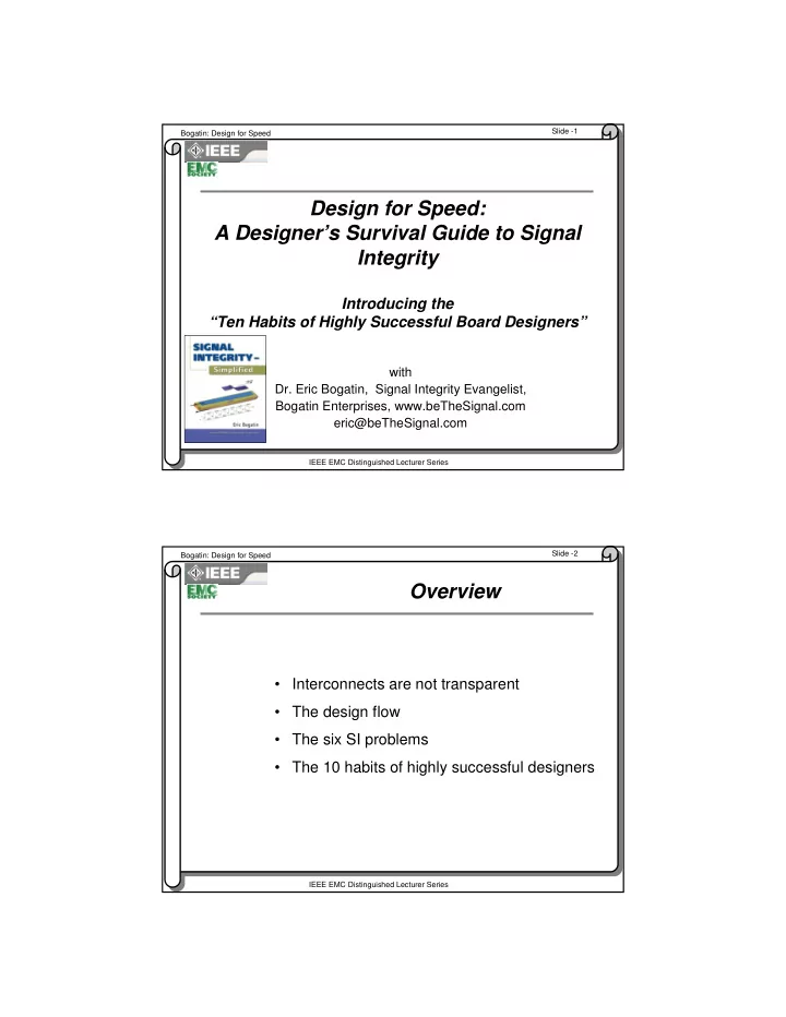

Slide -1 Bogatin: Design for Speed Design for Speed: A Designer’s Survival Guide to Signal Integrity Introducing the “Ten Habits of Highly Successful Board Designers” with Dr. Eric Bogatin, Signal Integrity Evangelist, Bogatin Enterprises, www.beTheSignal.com eric@beTheSignal.com IEEE EMC Distinguished Lecturer Series Slide -2 Bogatin: Design for Speed Overview • Interconnects are not transparent • The design flow • The six SI problems • The 10 habits of highly successful designers IEEE EMC Distinguished Lecturer Series
Slide -3 Bogatin: Design for Speed Interconnects are NOT Transparent 3 inch long PCB Trace receiver receiver driver Signal Integrity Engineering is about how the electrical properties of the interconnects screw up the beautiful, pristine signals from the chips, and what to do about it. IEEE EMC Distinguished Lecturer Series Slide -4 Bogatin: Design for Speed Why Interconnect are Not Transparent: The Most Important Signal Integrity Problems ��� No loss, after 12 inches 1. Reflection noise ��� ��������������� ��� FR4 loss, after 12 inches ��� 2. Cross talk ��� ��� ��� ��� ��� ��� ��� ��� ��� ��� 3. Ground (and power) bounce ���������� 4. Losses (@ Gbps) 5. Rail collapse, voltage droop, power supply Z PDN Vdd noise Z chip R 6. EMI IEEE EMC Distinguished Lecturer Series
Slide -5 Bogatin: Design for Speed Hope Can’t be Part of the Design Strategy in High-Speed Products IEEE EMC Distinguished Lecturer Series Slide -6 Bogatin: Design for Speed Ultimate Design Process • Come up with the Design • Model every element of the system: � Uniform regions with 2D field solver � Non uniform regions with 3D field solver • Simulate all pieces and interactions of the system � Circuit simulator � Electromagnetic simulator • Verify performance to specs • Optimize design to balance cost, schedule, risk, performance IEEE EMC Distinguished Lecturer Series
Slide -7 Bogatin: Design for Speed A Practical Design Process • Design with good habits that result in a robust design � Watch out for the six problems � Establish design guidelines (habits habits) to minimize the problems based on their root cause � Rely on your intuition to guide you in design tradeoffs � Minimize risk using appropriate analysis tools given the budget: expertise, $$, time � Use each design as an opportunity to move up the learning curve “… “… the more you know, the luckier you get the more you know, the luckier you get” ” IEEE EMC Distinguished Lecturer Series Slide -8 Bogatin: Design for Speed The Ten Habits of Highly Successful Board Designers 1. Design all interconnects as controlled impedance 2. Space out signals as far as possible 3. Don’t cross the return current streams 4. Do not allow signals to cross gaps in return planes 5. Use return vias adjacent to EVERY signal via 6. Keep via stubs short 7. Use loosely coupled differential pairs, with symmetrical lines 8. Use multiple power and ground planes on adjacent layers with thin dielectric between them 9. Use shortest surface traces possible for decoupling capacitors 10. If you don’t use SPICE to simulate the impedance profile of the decoupling capacitors, per power/gnd pin pair, use 2 each of 1 uf, 0.1 uf, 0.01 uf and 0.001 uf, located in proximity to device. IEEE EMC Distinguished Lecturer Series
Slide -9 Bogatin: Design for Speed Habit #1: Design All Interconnects As Controlled Impedance Controlled impedance structures twisted pair microstrip embedded stripline asymmetric coplanar coax microstrip stripline • Use uniform transmission lines to a target value ~ 50 Ohms • Keep the instantaneous impedance the signal sees, constant • Manage reflections at ends with termination scheme • Use a linear topology, avoid branches IEEE EMC Distinguished Lecturer Series Slide -10 Bogatin: Design for Speed Habit #2: Space Out Signals As Far As Possible � ���#!�����$�%&�'���������� ���� ���� Microstrip ���� Stripline ���� When s > 2 x w, NEXT < 2% ���� � � � � � � � � � � �� ����������� �!���������" For worst case NEXT in a bus, keep NEXT < 2% Design separation > 2 x w, MS or SL IEEE EMC Distinguished Lecturer Series
Slide -11 Bogatin: Design for Speed Habit #3: Don’t Cross The Return Current Streams • Re-calibrate your intuition about ground � Return path for signals GROUND � Return path for power • Never forget: If current flows in “ground”, there will be a voltage drop due to � I x R � L x dI/dt • Ground bounce: cross talk between signal lines with overlapping return currents � Most important design guideline: “Don’t cross the streams!” � Avoid overlap of return currents IEEE EMC Distinguished Lecturer Series Slide -12 Bogatin: Design for Speed Habit #4: Do Not Allow Signals To Cross Gaps In Return Planes Don’t route signals between split planes But if you do… - route signal layer close to continuous Vss - far from split plane layer 2.4v • Problems: signal � Reflection noise Vss 1.8v � Ground bounce � EMI signal Vss IEEE EMC Distinguished Lecturer Series
Slide -13 Bogatin: Design for Speed Habit #5: Use Return Vias Adjacent To EVERY Signal Via Voltage between Peak noise ~ 7% the planes Example courtesy of Sigrity 1 v signal in, RT = 0.1 nsec 300 mils away � � � � %&(�)���� � � � � 2% XTK @ 0.1 nsec rise time � � � � � � � � � � � � � � � � � � � � � � � � � � � � � � IEEE EMC Distinguished Lecturer Series Slide -14 Bogatin: Design for Speed Ideal Return Via Configuration to Minimize Ground Bounce Minimizes the spreading of the return currents from each via Ideal: A Good Habit: Reduces the spreading of the return currents from each via Worst case: Will cause ground bounce, inject “long range” noise in the plane Problem for very low noise boards IEEE EMC Distinguished Lecturer Series
Slide -15 Bogatin: Design for Speed Habit #6: Keep Via Stubs Short Top stub Bottom stub C via ~ 5 fF/mil IEEE EMC Distinguished Lecturer Series Slide -16 Bogatin: Design for Speed How to Avoid Via Stub Discontinuities? • Only use top layer to bottom layer vias- no stubs • Restrict layer transitions from near top to near bottom � From top layer to near bottom layer � From near bottom layer to near top layer • Use blind or buried vias • Back drill long stubs • Design stack up for thinner board • Try to keep via stubs < 60 mils long back drilled IEEE EMC Distinguished Lecturer Series
Slide -17 Bogatin: Design for Speed Habit #7: Use Loosely Coupled Differential Pairs, With Symmetrical Lines Higher Interconnect Density Common Noise rejection Lower Conductor Loss Thinner Dielectric tight loose Sweet spot s ~ 2w IEEE EMC Distinguished Lecturer Series Slide -18 Bogatin: Design for Speed Habit #8: Use Multiple Power And Ground Planes On Adjacent Layers With Thin Dielectric Between Them A h 0 . 225 pF / in ε 0 = A C Dk = ε 0 h Dk ~ 4 C = 1 h in mils, C/A in nF/inch 2 A h h = 3 mils, C/A = 0.3 nF/in 2 In 10 sq inches, C planes ~ 3 nF On-chip capacitance ~ 300 nF Thin dielectric provides low spreading inductance between decoupling capacitors and packages: - Near the surfaces - Multiple layers in parallel IEEE EMC Distinguished Lecturer Series
Slide -19 Bogatin: Design for Speed Habit #9: Use Shortest Surface Traces Possible For Decoupling Capacitors 2 1 4 3 3 1. Capacitor trace inductance 2. Via inductance to the planes 3. Spreading inductance in the planes 0402 4. Package mounting inductance For 3 mil thick dielectric to top plane: ~ 100 pH/sq For 10 mil thick dielectric to top plane: ~ 320 pH/sq w = 20 mils w = 40 mils Len = 120 mils Len = 60 mils IEEE EMC Distinguished Lecturer Series Slide -20 Bogatin: Design for Speed Habit #10: If you don’t use SPICE to simulate the impedance profile of the decoupling capacitors, per power/gnd pin pair, use 2 each of 1 uf, 0.1 uf, 0.01 uf and 0.001 uf, located in proximity to device. -�����#������.� ��������/0�� ��� 8 each of 1 uF • Assumptions: � � 250 mA per Target impedance for ¼ A per power/gnd pin pair power/gnd pin pair VRM ���� � > 10 inch planes, with 4 mil thick dielectric ���� � ESL of 2 nH per planes 2 each of 1 uF, 0.1 uF, 0.01 uF, 0.001 uF capacitor � On-chip capacitance < ���� 5 nF per power/gnd ��� ��� ��� ��� ��� ��� ��� pin pair �!�*��+, … lower ESL is always a more robust PDN IEEE EMC Distinguished Lecturer Series
Recommend
More recommend