Contents So what is it about ? Motivation Why Chips stop working - PDF document
How to destroy your ASIC:A beginner's guide 2/21/2012 Spoiler Alert ! What this presentation is NOT about Burn Baby Burn ! How to destroy your ASIC: A beginners' guide Diptyajit Choudhury & Pramod Ghimire Student lecture : ETI135 MS in System
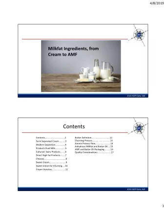
How to destroy your ASIC:A beginner's guide 2/21/2012 Spoiler Alert ! What this presentation is NOT about Burn Baby Burn ! How to destroy your ASIC: A beginners' guide Diptyajit Choudhury & Pramod Ghimire Student lecture : ETI135 MS in System on Chip (1 st year) LTH, Sweden 21 February 2012 Diptyajit Choudhury & Pramod Ghimire 2/46 Contents So… what is it about ? � Motivation Why Chips stop working � Electromigration Different reasons that we � Hot Carrier effects have collected! � Electro Static Discharge Few of them are chip level factors � CMOS Latchup � Clock Skew Others are external to the chip design � Heat Sink And most importantly, how � Power Supply to avoid or correct them 21 February 2012 Diptyajit Choudhury & Pramod Ghimire 3/46 21 February 2012 Diptyajit Choudhury & Pramod Ghimire 4/46 Diptyajit Choudhury & Pramod Ghimire 1
How to destroy your ASIC:A beginner's guide 2/21/2012 • A matter of decades from initial design to Time tapeout • Typically more than a year, even for small university projects • Non recurrent Engineering costs : Grand How to destroy your ASIC: A beginners' guide Money total [USD] 12,991,904 • Recurring Cost per unit : [USD] 25.98 MOTIVATION http://www.dz.ee.ethz.ch/?id=1592 21 February 2012 Diptyajit Choudhury & Pramod Ghimire 5/46 21 February 2012 Diptyajit Choudhury & Pramod Ghimire 6/46 Real life Cases � Pentium SRT Division Bug : $0.5 billion loss to Intel � Mercury Space Probe : Veered off course due to a failure to implement distance measurement in correct units. � Ariane 5 Flight 501 failure : Internal sw exception during � Ariane ‐ 5 Flight 501 failure : Internal sw exception during data conversion from 64 bit floating point to 16 bit signed How to destroy your ASIC: A beginners' guide integer value led to mission failure. � The corresponding exception handling mechanism contributed ELECTROMIGRATION to the processor being shutdown (This was part of the system specification). Subir Roy : ASPDAC / VLSI 2002 ‐ Tutorial on "Functional Verification of SoCs" 21 February 2012 Diptyajit Choudhury & Pramod Ghimire 7/46 21 February 2012 Diptyajit Choudhury & Pramod Ghimire 8/46 Diptyajit Choudhury & Pramod Ghimire 2
How to destroy your ASIC:A beginner's guide 2/21/2012 Illustration It can Electromi The cause gration is physics of opens a process electromi and involving gration is shorts in the net very circuit movemen complex WHAT interconn t of metal WHY and is WHAT IS EFFECTS ections in atoms DOES IT related to IT ? IT ? DOES IT DOES IT mixed ‐ mixed ‐ under the OCCUR ? materials HAVE ? signal ICs, influence propertie even of s such as under electron grain normal flow and boundary, operating temperat vacancy condition ure. flux, etc. s. http://people.ccmr.cornell.edu/~ralph/projects/emig_movies/ 21 February 2012 Diptyajit Choudhury & Pramod Ghimire 9/46 21 February 2012 Diptyajit Choudhury & Pramod Ghimire 10/46 Simulation results IBM research in 1970 � 4% copper added in aluminium increased the life of the interconnect by the factor of 70. � Until the late 1990s, IBM used aluminum/copper (4%) allo to interconnect comp ter circ its (4%) alloy to interconnect computer circuits. � copper-based processes continue to be the state of the art for the semiconductor industry today. The original resistance of the wire was 2.88ohm. A constant 0.1mA testing current was used for simulation. After 200 hours’ stress at 250° C, the change of wire resistance was 1.9 http://www ‐ tr.watson.ibm.com/journal/50th/devices/ames.html ohms, a percentage degradation of 66%. 21 February 2012 Diptyajit Choudhury & Pramod Ghimire 11/46 21 February 2012 Diptyajit Choudhury & Pramod Ghimire 12/46 Diptyajit Choudhury & Pramod Ghimire 3
How to destroy your ASIC:A beginner's guide 2/21/2012 Avoiding Electro Migration How to destroy your ASIC: A beginners' guide HOT CARRIER EFFECTS Reference: Peter slide on wire, slide number 9”Digital IC Course” 21 February 2012 Diptyajit Choudhury & Pramod Ghimire 13/46 21 February 2012 Diptyajit Choudhury & Pramod Ghimire 14/46 What is it ? Mars Rover Case study � Hot ‐ carrier ‐ induced degradation of MOS transistors is caused by the injection of high ‐ energy electrons and holes into the gate oxide region near the drain region near the drain. � The degradation is in the form of localized oxide charge trapping and/or interface generation, which gradually builds up and permanently changes the oxide ‐ interface charge distribution PMOS Hot Carrier Aging lifetime is two orders of magnitude than corresponding NMOS 21 February 2012 Diptyajit Choudhury & Pramod Ghimire 15/46 21 February 2012 Diptyajit Choudhury & Pramod Ghimire 16/46 Diptyajit Choudhury & Pramod Ghimire 4
How to destroy your ASIC:A beginner's guide 2/21/2012 PARAMETER DEGRADATION How to destroy your ASIC: A beginners' guide ELECTRO STATIC DISCHARGE 21 February 2012 Diptyajit Choudhury & Pramod Ghimire 17/46 21 February 2012 Diptyajit Choudhury & Pramod Ghimire 18/46 Electro…what ? Why ? 21 February 2012 Diptyajit Choudhury & Pramod Ghimire 19/46 21 February 2012 Diptyajit Choudhury & Pramod Ghimire 20/46 Diptyajit Choudhury & Pramod Ghimire 5
How to destroy your ASIC:A beginner's guide 2/21/2012 Should we be concerned ? Electro Static Discharge � A shunt device to discharge positive polarity transients � A shunt device to discharge negative polarity transients � A series element for current limiting Reference: Peter slides on interconnection slide number 18 21 February 2012 Diptyajit Choudhury & Pramod Ghimire 21/46 21 February 2012 Diptyajit Choudhury & Pramod Ghimire 22/46 Area ‐ Efficient CMOS Output Buffer Electro Static Discharge � There are one PTLSCR Device (PMOS trigger lateral SCR) and one NTLSCR device used to effectively protect CMOS Electrostatic discharge can happen anytime a charged output buffer against the four ‐ mode ESD conductive object approaches another conductive object. stresses. Features desirable in portable devices for ESD protection � In PTLSCR (NTLSCR) structure. there is � Capacity to handle high peak ESD currents a shortchannel thin ‐ oxide PMOS (NMOS) device inserted into the lateral SCR � Ability to remain undamaged by repetitive ESD strikes � Abili i d d b i i ESD ik structure. � Minimal size � This PMOS (NMOS) device with its � Minimal reverse leakage current drain made across the junction between N ‐ well and P ‐ substrate is used to Source: http://www.semtech.com/circuit-protection/What-is-ESD-Protection/index.html triggered on the lateral SCR structure at its drain snapback ‐ breakdown voltage under the ESD ‐ stress conditions. 21 February 2012 Diptyajit Choudhury & Pramod Ghimire 23/46 21 February 2012 Diptyajit Choudhury & Pramod Ghimire 24/46 Diptyajit Choudhury & Pramod Ghimire 6
How to destroy your ASIC:A beginner's guide 2/21/2012 Results : Evaluation 21 February 2012 Diptyajit Choudhury & Pramod Ghimire 25/46 21 February 2012 Diptyajit Choudhury & Pramod Ghimire 26/46 Illustration How to destroy your ASIC: A beginners' guide CMOS LATCHUP Reference:Digital Integrated Circuits, A design Perspective , second edition, Rabaey ,Chandrakasan, Nikolic,page no 116 21 February 2012 Diptyajit Choudhury & Pramod Ghimire 27/46 21 February 2012 Diptyajit Choudhury & Pramod Ghimire 28/46 Diptyajit Choudhury & Pramod Ghimire 7
How to destroy your ASIC:A beginner's guide 2/21/2012 Description Reduction � To avoid Latchup, the resistance R well and R psubs should be � The combination of the wells and substrates results in the minimized. formation of parasitic n ‐ p ‐ n ‐ p structures � According to the book, in recent years, process innovations � According to the book in recent years process innovations � Triggering these thyristor like devices leads to a shorting of the V DD and improved design techniques have all but eliminated the and V SS lines. risk for Latchup. � Resulting in a destruction of the chip, or at best a system failure that can only be resolved by a power ‐ down 21 February 2012 Diptyajit Choudhury & Pramod Ghimire 29/46 21 February 2012 Diptyajit Choudhury & Pramod Ghimire 30/46 What is it ? � Difference in clock signal arrival times across the chip is called clock skew � Clocking sequentially ‐ adjacent registers on the same edge of a high skew clock can potentially high ‐ skew clock can potentially cause timing violations or even How to destroy your ASIC: A beginners' guide functional failures. Probably this is one of the largest sources of design failure in an ASIC. CLOCK SKEW Reference:http://www.eetimes.com/ContentEETimes/Doc uments/EDADesignline/201201/Chapter2_Clocks_Re sets ‐ 04.pdf 21 February 2012 Diptyajit Choudhury & Pramod Ghimire 31/46 21 February 2012 Diptyajit Choudhury & Pramod Ghimire 32/46 Diptyajit Choudhury & Pramod Ghimire 8
Recommend
More recommend
Explore More Topics
Stay informed with curated content and fresh updates.

