CLIC Vertex Detector R&D Sophie Redford on behalf of the CLIC - PowerPoint PPT Presentation
CLIC Vertex Detector R&D Sophie Redford on behalf of the CLIC Detector and Physics Collaboration CLIC - a collider for the future Linear electron-positron collider s = 3 TeV (staged construction) High luminosity: 10 34 cm
CLIC Vertex Detector R&D Sophie Redford on behalf of the CLIC Detector and Physics Collaboration
CLIC - a collider for the future • Linear electron-positron collider • √ s = 3 TeV (staged construction) • High luminosity: 10 34 cm -2 s -1 • Small bunch size: σ xyz (40 nm, 1 nm, 44 µm) • Beam structure: 156 ns 312 bunches per train 2
Detector environment • Beamstrahlung creates high particle rate ‘beam induced backgrounds’ - most at low angle, low p T , constrained by B field • Inner radius of vertex detector restricted by particle density Maximum occupancy including safety factor 5: 1.9% per pixel in the barrel layers 2.9% per pixel in the forward layers 3
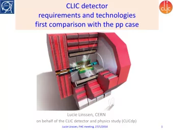
The CLIC detector Precision physics in a challenging environment: broad programme of R&D Highly granular particle flow calorimetry, using tungsten absorber 5.5 m diameter cryostat for superconducting solenoid, B field 4-5 T Instrumented steel return yoke Complex forward region Detector challenges at CLIC, S. Lukic, Monday 17:00 4
Vertex detector requirements l a o G Efficient tagging of heavy quarks through a precise determination of displaced vertices • Single point resolution of 3 µm • Material budget of < 0.2% of a radiation length per layer • No active cooling elements - use forced air flow cooling • Limit the power dissipation to Multi-layer barrel and endcap pixel detectors 50 mW/cm 2 in sensor area ‣ 560 mm in length • Hit time slicing of 10 ns ‣ Barrel radius from 30 mm to 60 mm 5
Olympic programme of R&D Readout Thin assemblies Supports Powering Cooling 6
Geometry optimisation studies Double-sided Single-sided Comparison of 5 single-sided layers layers layers and 3 double-sided layers • Similar flavour tag performance for two considered layouts • Increasing the material has a larger impact than the layout Dijets at 200 GeV Dijets at 200 GeV 1 1 Misidentification eff. Misidentification eff. Average number of layers Charm Background Charm Background 8 double_spirals double_spirals_v2 -1 -1 10 10 spirals double_spirals 6 -2 -2 10 10 4 CDR LF Background LF Background spirals double_spirals double_spirals_v2 2 -3 -3 10 10 spirals double_spirals double_spirals 0 double_spirals/spirals double_spirals_v2/double_spirals 0 20 40 60 80 0.5 0.6 0.7 0.8 0.9 1 0.5 0.6 0.7 0.8 0.9 1 Charm Background 1.4 [ ] 1.1 ! ° Charm Background LF Background LF Background 1 1.2 0.9 1 0.8 0.5 0.6 0.7 0.8 0.9 1 0.5 0.6 0.7 0.8 0.9 1 7 Beauty eff. Beauty eff.
Thin sensor assemblies • Hybrid planar pixel technology • Ultimate goal: 50 µm sensor on 50 µm ASIC • 25 µm pitch • Thin edge sensors using Through-Silicon-Vias • 60 µm hole diameter • Wafer thinned to 120 µm • 5 µm copper layer for TSV 50 µm thick silicon wafer TSVs: • Vertical electrical connection - no wire bonds • Sensors buttable on all sides - better tiling 8 First Medipix3 Image using TSV
Testbeam analysis 50 µm sensor • Thin sensors (50 - 300 µm) bonded to normal Timepix chips • One 100-on-100 µm assembly 750 µm Timepix • Data recorded at DESY: 5.6 GeV electron beam Track position: cluster size 4 Track position: cluster size 2 C04-W0110 Oct13 Efficiency 0.995 0.99 0.985 0.98 0.975 0.97 Preliminary 0.965 0.96 0.955 380 385 390 395 400 405 410 415 Threshold 50 µm thick sensor Efficiency 99.2% at operating threshold 100 µm thick sensor - low charge sharing 9
Two-hit cluster resolutions Digital centroid • 2 hit clusters no calibration DigitalCentroid Tracking resolution of telescope ~3.5 µm 20000 Constant Constant 1.28e+04 1.28e+04 5.90e+01 5.90e+01 ± ± 18000 • Mean Mean -0.0002745 -0.0002745 0.0000182 0.0000182 ± ± Digital centroid method effective due to low charge sharing 16000 Sigma Sigma 0.005334 0.005334 ± ± 0.000016 0.000016 14000 Projection of (1,2) 12000 Number of hits 10000 Constant Constant 3897 3897 ± ± 29.9 29.9 6000 Sigma Sigma 0.005214 0.005214 0.000026 0.000026 ± ± 8000 5000 Resolutions include tracking resolution Preliminary 6000 4000 4000 Project 3000 2000 0 2000 -0.1 -0.05 0 0.05 0.1 Y residual (mm) 1000 0 Charge weighting (eta corr.) 0 0.01 0.02 0.03 0.04 0.05 0.06 Track y position (mm) 2 hit clusters no calibration EtaCorrection 22000 Constant Constant 1.412e+04 1.412e+04 6.570e+01 6.570e+01 ± ± • 20000 Eta correction method of charge weighting best Mean Mean -0.000255 -0.000255 0.000016 0.000016 ± ± 18000 Sigma Sigma 0.004809 0.004809 ± ± 0.000015 0.000015 resolution: take into account non-linearities in 16000 charge sharing 14000 12000 • 10000 Unfolding the tracking resolution gives a single 8000 Preliminary point hit resolution of 3.3 µm for 2 hit clusters 6000 4000 2000 100 µm thick sensor 0 10 -0.1 -0.05 0 0.05 0.1 Y residual (mm)
Sensor calibration c • Sources and X-ray fluorescence 241 Am 60 keV Calibrate TOT values by y = ax + b − x − t measuring response to photons of known energy 241 Am 26.2 keV Indium 24 keV • Accounts for non-linearities 09 Cd: 22.9 keV a • Calibration aligns Landau’s b Brass 8.1 keV c and improves the resolution: t 55 Fe: 5.8 keV 4.8 µm → 4.7 µm Resolutions include tracking resolution 2 hit clusters global calibration EtaCorrection No calibration Global calibration 22000 Cluster size 1 Cluster size 1 Constant Constant 1.441e+04 1.441e+04 6.718e+01 6.718e+01 ± ± 0.14 0.07 Cluster size 2 Cluster size 2 20000 Mean Mean -0.0002513 -0.0002513 0.0000162 0.0000162 ± ± Cluster size 3 Cluster size 3 0.12 0.06 18000 Sigma Sigma Cluster size 4 Cluster size 4 0.00471 0.00471 ± ± 0.00001 0.00001 16000 0.1 0.05 14000 0.08 0.04 12000 Calibration 10000 0.06 0.03 8000 Preliminary 0.04 0.02 6000 4000 0.02 0.01 2000 0 0 0 0 1000 2000 3000 4000 5000 0 20 40 60 80 100 120 140 -0.1 -0.05 0 0.05 0.1 Energy (keV) Y residual (mm) TOT value 11
Readout ASIC: CLICpix • The CLICpix ASIC: a fast, low power readout chip with 25 µm pitch • Implemented in 65 nm CMOS technology • 4-bit time and energy measurements for each pixel • Supports power-pulsing and data compression FPGA Board Chip Board 64 x 64 25 µm pixels 3 mm 12 1.85 mm
CLICpix characterisation TOT gain distribution 0.35 • Time Over Threshold gain distribution • Pixels 1-64 Uniform gain across the whole matrix • 0.3 Gain variation is 4.2% r.m.s. (for nominal feedback current) 0.25 Pixels 1-64 • Matrix equilisation • Calibrated spread is 0.89 mV (about 22 e - ) across the whole matrix • (Expect a signal of ~thousands of electrons in 50 µm sensor) 13
Power-pulsing strategy • Power pulse CLICpix ASIC to achieve dissipation <50 mW/cm 2 in the sensor area • Analog electronics can be turned off: 2 W/cm 2 → 2 mW/cm 2 • Digital electronics in idle except during readout: 100 mW/cm 2 → 13 mW/cm 2 Train Bunch 20µs 20µs Analog Chip [1:12] ON OFF ON Digital Chip [1] ON Idle Read Out Idle ON Digital Chip [2] ON Idle Read Out Idle ON 20/12 ms 20/12 ms 20/12 ms Digital Chip [12] ON Idle Read Out Idle ON Read Out 360 mW/cm 2 Turned OFF ON 2 W/cm 2 OFF ON 100 mW/cm 2 Idle 8 mW/cm 2 14
Power delivery • Power ladders from each end of the barrel: ‣ constant current sources, low dropout regulators, silicon capacitors Vertex barrel 24 cm 1 cm P o w e r i n P o w e r i n 1 cm Power each half a ladder CLICpix Ladders Material budget: • Aluminium flex cables and silicon capacitors reduce material • Powering adds 0.1% X 0 per layer. Projected: < 0.05% X 0 15
Power-pulsing lab tests Al Flex Cable Dummy load Back-end cables Controlled current source V load Analogue: ∆ V = 16 mV 1.2 V • Voltage drop < 20 mV 2 A per chip • Measured average power 5.3 V I load for 1 ASIC V Cap dissipation < 10 mW/cm 2 Digital: • Particular case t on = 20 μ s Measured average power dissipation < 35 mW/cm 2 1.4 V Total dissipation: < 50 mW/cm 2 Analogue results 16
Air-flow cooling • Total heat load after power-pulsing ~470 W • Cooling provided by forced air-flow: ‣ Dry air cooling at 0°C ‣ Low material: radiation length of air ~310m Cool air Warm air 17
Air-flow simulations • Mass flow: 19.9 g/s • Avg. velocity in barrel: 6.3 m/s • Silicon temperature below 40 o C • Conduction not taken into account 18
Mechanical support structures • Develop and characterise low-mass carbon-fibre structures • Stave dimension 1.8 mm*26 mm*280 mm Skin stave • Goal material per layer: 0.05% X 0 Cross braced staves Full sandwich stave Rohacell core (PMMA) Honeycomb core (Nomex and Carbone) Mass 3.74 g 3.45 g 3.08 g 2.74 g 1.76 g X/X 0 0.121% 0.112% 0.118% 0.068% 0.051% 19
Stave mechanical characterisation • Measure the flexural stiffness (resistance to bending) of the staves over span of 180 mm Measurements 6.95 N/mm 2.24 N/mm 3.3 N/mm 2.96 N/mm 2.23 N/mm Simulations 6.95 N/mm 2.35 N/mm - - 2.30 N/mm Next: measure the amplitude of stave vibration in air flow 20
Thermo-mechanical test bench Air flow • Measure wind speeds, stave temperatures, stave vibrations • Allows validation of simulations Thermal camera Simulation 90 deg. 0 deg. 21
Recommend
More recommend
Explore More Topics
Stay informed with curated content and fresh updates.
