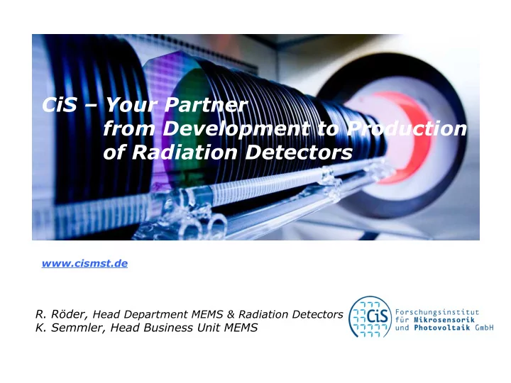

CiS – Your Partner from Development to Production of Radiation Detectors www.cismst.de R. Röder, Head Department MEMS & Radiation Detectors K. Semmler, Head Business Unit MEMS
OUTLINE Orgin/History, Enterprise structure, Staff, … • Some facts about CiS • CiS products and services • CiS experiences in the field of radiation detectors • CiS offers Technology capabilities and capacity, … • Actual working packages Detector development activities, R&D batches • Outlook R&D plans, Road map 2 PIXEL2010 CiS R. Röder 9 September, 2010
Location Erfurt Industrial Area southeast X-FAB CiS X-FAB 3 PIXEL2010 CiS R. Röder 9 September, 2010
Some facts about CiS Foundation of unite CiS e.V. • 1992 CiS Orgin: by interested persons and enterprices in the field of microelectronics, MEMS, Optoelectronics and so on 1993 Foundation of CiS GmbH non-profit company, 100% ownerchip CiS e.V. with laboratories / clean rooms in the Thesys buildings 1996 DIN EN ISO 9001 certification • Career: 1997 Start of Prototyping of Silicon Radiation Detectors 1999 CiS Institut for Microsensors gGmbH Start of Prototyping of Silicon Radiation Detectors 2001 New Location in Technology Center AZM 2004 Foundation of CiS Solar Center and Solar Test Lab CiS Resaerch Institut for Microsensors and Photovoltaics GmbH 2008 Best Supplier Award ATLAS PIXEL 2009 CMS Gold Awards 4 PIXEL2010 CiS R. Röder 9 September, 2010
CiS in Numbers 2009 Yearly financial volume 9.4 Mio €, 92 employees (unlimited) Public sector and strategic programmes 51 % Industrial contracts R&D 35 % Industrial contracts (components) 14 % Microintegration Clean room: 70 m 2 acc10 (high temperature processes, resist processing lab, ...) approx. 200 m 2 acc100 (test lab, assembly, ...) 200 m 2 acc 10,000 (services, assembly, packaging ) 5 PIXEL2010 CiS R. Röder 9 September, 2010
CiS Research Institut for Microsensors and Photovoltaics Enterprise structure CiS e.V. Scientific Council CiS Board Services Product groups Design, Simulation, Layout MEMS Wafer processing Supervisory Board Assembly+Packaging, MOEMS Test+Analysis, Photovoltaik Calibration lab R&D Services & PV g n s i e s c o p r e r a f w a r o l s wafer processing and Packaging testing & analysis 6 PIXEL2010 CiS R. Röder 9 September, 2010
CiS Organisation Approx. 120 employees (2009) Business Units 90 Scientists / engineers Solar Centre Radiation Detectors 10 apprenticeships MOEMS MEMS Students (Diplom, Masters, PhD) Simulation / Design Technology Waferprocessing Departments Assembly / Packaging Test & Analytics MOEMS System MEMS Photovoltaics 7 PIXEL2010 CiS R. Röder 9 September, 2010
CiS Main Products PIN-Diode Arrays Emitter-Receiver-Modules Silicon Radiation Detectors Humidity Sensors MEMS 8 PIXEL2010 CiS R. Röder 9 September, 2010
Business Unit MEMS Department MEMS & Radiation Detectors MEMS Research and Development Programs Radiation 3D-MEMS Impedimetric Piezoresistive Detectors Sensorics Sensorics • single or double sided • Micro condensation • Cantilever • High stable pressure • Micro strip detectors sensors • Probe tips sensors • PIXEL detector • Force sensors • Dew point sensors • with excellent • n-in-n, n-in-p • In-line micro fluidic • Bi-stable long-term stability • DOFZ, epi-RD sensors zero power sensors • Small thermal and pressure hysteresis 9 PIXEL2010 CiS R. Röder 9 September, 2010
Business Unit MEMS In-house Departements MEMS Services for Industry Partners Development Research Production innovative and new sensor concepts Customer specific high precision sensor and technologies sensor solutions chips and systems • more than 20 funded • Small and midsize series production • Modelling , Simulation , Design research projects • Single and second-source supplier • Manufacturing departements • wafer processing for leading pressure instrument • Long-term and close relations manufacturers • dicing to MEMS / Sensor research • Unit process / process sequence or • assembly & and university institutes packaging complete processing (foundry) • test& calibration • Long-term and close relations • Continuous yield improvement and • Experienced project leader to University of Hamburg, quality management system in industrial, TU Dortmund, MPI HLL automotive Munich 10 and medical PIXEL2010 CiS R. Röder 9 September, 2010 engineering
Equipment Wafer Simulation & Design - 4inch wafer line, front and backside processing - Layout – CAD-Software - Lithography < 1μm - FEM-Simulation tools for - Lift-off resist system (single and double layer electrical, optical, mechanical & thermal solution) calculations - Under bump metalization e.g. ANSYS, COMSOL, ATLAS, ATHENA, TESCA - Spray-Coating for 3D-MEMS/MOEMS - SPICE-Simulations (HSPICE, CADENCE pSPICE) - Si-direct bonding, anodic bonding Test & Analytics Assembly and packaging - 8inch wafer prober - Automatic die bonder, + 4inch and 6inch front and backside wafer prober manual fine placer for flip-chip assembly - Opto-wafer-prober (e.g. OBIC) - Automatic ultra-sonic and thermosonic wire bonder - SIMS-analysis, SEM including EDX, AFM - Semiautomatic wire bonder - Optical and mechanical profilometer - Screenprinter and SMD-mounter, Automatic - Climate and temperature shock test chambers, dispenser Pressure cooker - Wafer dicing (e.g. Si, glass), precision dicing - Measurement techniques process e.g. CV, TVS, UBR, pin-hole, lifetime - Vapor-phase, hot bar, vacuum and laser soldering equipment 11 - Electroless Nickel Bumping like IZM standard PIXEL2010 CiS R. Röder 9 September, 2010 process
Wafer Processing Equipment • 4 inch some process steps already in 6 inch (capable), equipment partly 6 inch compatible • Silicon (FZ, CZ, n-typ, p-typ, epi, SOI, SF bonded wafer) High temperature facility • 6 inch capable, investment in quartz ware is necessary • dry and wet oxydation (O 2 ,HCl, H 2 O, /O 2 ) without organics ! • oxygen enrichment (DO, e.g. DOFZ) • diffusion and anneling steps (N 2 800…1200°C, H 2 …420°C) • diffusion by target gas LP-CVD (only 4 inch capable) • • silicon nitrid • high temperature oxid HTO • Poly-Silicon • low temperature oxid LTO (doped or undoped) • PE-CVD (only 4 inch capable) • silicon nitrid • silicon oxynitride • phosphorus silicate glass PSG – POCl 3 12 PIXEL2010 CiS R. Röder 9 September, 2010
Wafer Processing Equipment • Magnetron sputter facility (2x) Al, AlSi, AlSiTi, TiN, MoSi, other targets available (W,…) 4 inch → 6 inch capability require re-equip of wafer chuck etc. • RIE- and plasma etching equipment (only 4 inch capable) Wet benches: isotrop, anisotrop and electro-chemical etching • porousizing • Megasonic fine cleaning (only 4 inch capable) • Automatic coating & developing cluster for double-sided processing alignment precision rear to front side better than 5 µm for double side detector processing ~ 2 µm 6 inch capable Double-sided alignment and exposure facility BA/MA6 alignment precision rear to front side approx. 1 µm Silicon Fusion facilities BA/MA6 + SB6L 13 PIXEL2010 CiS R. Röder 9 September, 2010
Wafer Processing Equipment • Spray coating equipment for 3D-structuring • new own equipment developed → 6 inch capable • Goal: 3D pattering process with an optimized and highly conform spray-coating photoresist deposition which provides an improved pattern resolution and process stability. Commercial CiS spray spra ray coater coater CiS spray coater 14 PIXEL2010 CiS R. Röder 9 September, 2010
Wafer Processing Post-Processing Technology Modules Lift-off masks for UBM ▪ single-layer lift-off resist ▪ double-layer lift-off resist 15 PIXEL2010 CiS R. Röder 9 September, 2010
Wafer Processing Post-Processing Technology Modules • Electroless Nickel UBM Process • like IZM-process, licenced by IZM • optimized for regular array structures e.g. ATLAS PIXEL • 5 µm Ni und 60-80 nm Au 16 PIXEL2010 CiS R. Röder 9 September, 2010
NETWORK external services FZ Wafers ▪ Topsil (ingot, wafers as cut, dsp) ▪ additional qualified supplier ??? ▪ Okmetic (certificated supplier) Cz, MCz Epi layer Okmetic (certificated supplier) + ITME (R&D) ▪ Okmetic (certificated supplier) Wafer Polishing ▪ additional qualified supplier ??? Wafer Thinning + Polishing Okmetic (certificated supplier) + WaferWorld (first experience) ▪ additional qualified supplier ??? + Disco (first experience) CMP ZMN Ilmenau Fraunhofer Institute ENAS 17 PIXEL2010 CiS R. Röder 9 September, 2010
NETWORK external services Implantation Ion Beam Services (F + GB high dosis fascilities) → Boron, Phosphorus, Arsenic, … FZ Dresden-Rossendorf → high energy implantation → unusual dopands Au Metalization ifw Jena (very good experience in combination with lift-off Ti-Ni-Au UBM) DRIE/ICP ZMN Ilmenau 18 PIXEL2010 CiS R. Röder 9 September, 2010
Recommend
More recommend