Center for Electromagnetic Compatibility Industrial Advisory Board - PDF document
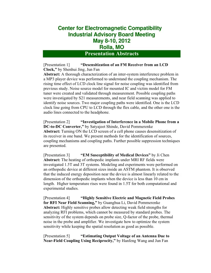
Center for Electromagnetic Compatibility Industrial Advisory Board Meeting May 8-10, 2012 Rolla, MO Presentation Abstracts [Presentation 1] Desensitization of an FM Receiver from an LCD Clock, by Shenhui Jing, Jun Fan Abstract: A thorough
Center for Electromagnetic Compatibility Industrial Advisory Board Meeting May 8-10, 2012 Rolla, MO Presentation Abstracts [Presentation 1] “Desensitization of an FM Receiver from an LCD Clock,” by Shenhui Jing, Jun Fan Abstract: A thorough characterization of an inter-system interference problem in a MP3 player device was performed to understand the coupling mechanism. The rising time effect of LCD clock line signal for noise coupling was identified from previous study. Noise source model for mounted IC and victim model for FM tuner were created and validated through measurement. Possible coupling paths were investigated by S21 measurements, and near field scanning was applied to identify noise sources. Two major coupling paths were identified. One is the LCD clock line going from CPU to LCD through the flex cable, and the other one is the audio lines connected to the headphone. [Presentation 2] “Investigation of Interference in a Mobile Phone from a DC-to-DC Converter,” by Satyajeet Shinde, David Pommerenke Abstract: Turning ON the LCD screen of a cell phone causes desensitization of its receiver in one band. We present methods for the identification of sources, coupling mechanisms and coupling paths. Further possible suppression techniques are presented. [Presentation 3] “EM Susceptibility of Medical Devices” by Ji Chen Abstract: The heating of orthopedic implants under MRI RF fields were investigated 1.5T and 3T systems. Modeling and experiments were performed on an orthopedic device at different sizes inside an ASTM phantom. It is observed that the induced energy deposition near the device is almost linearly related to the dimension of the orthopedic implants when the device is less than 10 cm in length. Higher temperature rises were found in 1.5T for both computational and experimental studies. [Presentation 4] “Highly Sensitive Electric and Magnetic Field Probes for RFI Near Field Scanning,” by Guanghua Li, David Pommerenke Abstract: Highly sensitive probes allow detecting weak field strengths for analyzing RFI problems, which cannot be measured by standard probes. The sensitivity of the system depends on probe size, Q-factor of the probe, thermal noise in the probe and amplifier. We investigate how to optimize the system sensitivity while keeping the spatial resolution as good as possible. [Presentation 5] “Estimating Output Voltage of an Antenna Due to Near-Field Coupling Using Reciprocity,” by Hanfeng Wang and Jun Fan
Abstract: The RF noise voltage received by an antenna due to near-field coupling is estimated using reciprocity, where the multiple scattering effect is neglected. This could be used for certain RF interference studies where the dominant noise mechanism is near-field coupling. [Presentation 6] “Modeling of Roughness of PCB Traces,” by Ji Chen Abstract: The analysis of conductor loss for a transmission line with arbitrary cross-section and periodic surface roughness along the propagation direction is presented in this paper. The frequency dependent skin-effect and proximity are both considered in the analysis. The per-unit-length impedance is extracted by assuming smooth metal surface. Modified surface impedance account for the periodic metal surface roughness is then incorporated for high-frequency correction. The first step is to extract a series per-unit-length impedance as a function of frequency without considering the skin-depth and current crowding effect. The compact 2D-FDTD solver is used to model the entire cross-sectional geometry (possibly inhomogeneous) assuming metals are perfect electric conductor. To analyze the skin-depth as well as the current crowding effect, the obtained electromagnetic field distribution on the surface is then used as the boundary condition to analyze the current distribution inside the conductor; the conductor-only model is then built in the 2D-FDTD solver with finer meshes to capture the current redistribution as a result of finite conductivity. The equivalent surface impedance of the conductor is therefore obtained with a scale factor extracted as a function of the location on the circumference of the conductor. Upon the series per-unit-length impedance is solved, the fine features of the metal surface roughness is modeled as periodic protrusions.. The active reflect coefficient is calculated to obtain the surface impedance for the rough metal, served as the normalized value in the scaled surface impedance function. [Presentation 7] “PCB Conductor Surface Roughness as an Effective Dielectric Layer,” by Koledintseva Marina Abstract : A simple model to substitute conductor surface roughness in printed circuit boards by a layer with an effective material lossy dielectric) is proposed and tested using the 2D finite-element method (FEM) electromagnetics numerical simulations. The results of numerical modeling of a multilayered structure corresponding to a stripline transmission line with substituted roughness are compared with the experimental results obtained on a TRL-calibrated test vehicle with significant roughness on conductors made of three types of copper foils: a standard (STD)-roughness, very-low-profile (VLP), and hyper-very-low-profile (HVLP) foils. [Presentation 8] “Estimation of Driver Jitter Due to Power/Ground Noise,” by Chunchun Sui and Jun Fan Abstract: The transfer function of supply voltage fluctuation to jitter is analytically derived in closed form expressions for a single-ended buffer. The analytic transfer function is derived from the linear differential equation obtained
from asymptotic linear inverter I-V curves. The transfer functions are validated by comparison with HSpice simulations, and the estimated jitter is compared to simulated jitter in eye diagram with single-frequency and multi-tone supply noise. [Presentation 9] “Fast Admittance Computation for TSV Arrays,” by Dazhao Liu and Jun Fan Abstract: A fast method to calculate the admittance matrix of Through Silicon Vias (TSVs) is proposed in this talk. The silicon dioxide layers are equivalently modeled using the bound charge on the conductor surfaces as well as on the dielectric interface between the silicon dioxide and the silicon regions. Unknown surface densities of both the free and bound charge are expanded using the axial harmonics. Galerkin’s method is then applied to obtain the capacitance and conductance matrices. The proposed method is validated with a full-wave 2D cross-sectional analysis tool for a typical TSV pair structure. Comparisons with popular closed-form expressions are also discussed. . [Presentation 10] “ EMI Analysis of DVI Link Connectors ,” by Soumya De, Yaojiang Zhang, Abhishek Patnaik, David Pommerenke, Chen Wang, Charles Jackson Abstract: In the Digital Visual Interface (DVI) the DVI connector is an important link. The discontinuities in the connector itself can convert differential signals to common mode which can further produce antenna mode currents causing EMI. The overall goal of the study is to analyze the DVI connector by quantifying the effects of the discontinuities in the connector and the return path of the currents. This is done in a step-by-step manner by first analyzing the port voltages along the discontinuities in the connector and then measuring the radiated field for EMI analysis. In this presentation, we will discuss the measurement strategies and the results. [Presentation 11] “Capacitance Calculation of TSVs Using an Integral Equation Method Based on Partial Capacitances,” by Hanfeng Wang, Al Ruehli, and Jun Fan Abstract: An integral equation method based on partial capacitances is used to extract the capacitance between two through-silicon-vias (TSVs). The unrealistic assumption of equal potential along the vertical interface of silicon dioxide (SiO 2 ) coating of TSVs in the analytical method has been removed by introducing unknown equivalent charge. The Galerkin’s method is used here to solve the unknown charge densities in the integral equation and thus, the capacitance between two TSVs can be efficiently calculated. The results are validated by comparing the extracted capacitances with commercial software based on the finite element method. The accuracy and efficiency have been demonstrated. [Presentation 12] “Modeling Vias Sharing a Common-Antipad with a Fast Hybrid Finite Element Method,” by Yaojiang Zhang and Jun Fan Abstract: Vias sharing a common-antipad is a typical PCB geometry. Effective models for this geometry can provide accurate estimation of signal propagation
Recommend
More recommend
Explore More Topics
Stay informed with curated content and fresh updates.
