C0MBINED TEXTURE-MICROSTRUTURE-PHASES- - PowerPoint PPT Presentation
C0MBINED TEXTURE-MICROSTRUTURE-PHASES- STRAINS-STRUCTURE-REFLECTIVITY ANALYSIS D. Chateigner, CRISMAT-ENSICAEN, Caen, France M. Morales, LERMAT-ENSICAEN, Caen, France L. Lutterotti, DME, Trento, Italy Goals: Obtain structure,
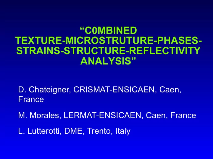
“C0MBINED TEXTURE-MICROSTRUTURE-PHASES- STRAINS-STRUCTURE-REFLECTIVITY ANALYSIS” D. Chateigner, CRISMAT-ENSICAEN, Caen, France M. Morales, LERMAT-ENSICAEN, Caen, France L. Lutterotti, DME, Trento, Italy
• Goals: – Obtain structure, microstructure, texture and residual stresses of polyphased thin structures by one step methodology – The analysis should not be limited by phase overlapping, strong texture or complex structures • How/Why ? -> Rietveld + ODF analysis by cyclic full pattern fitting – Textured non-destructible materials – Texture / Structure / Strains / Phases … parameters correlation – Final program: MAUD, developed inside the ESQUI European project
• Some examples: – Ferroelectric thin heterostructures: texture, structure, microstruct. – Nanocrystalline silicon thin films: texture, structure, anisotropic shapes – Amorphous silicon oxynitrides very thin films: Electron Density Profiles – Irradiated fluoroapatites: texture, phase, structure – Bi-based superconductor ceramics: texture, phase, structure, E. Guilmeau, poster VII-P4
Texture from Spectra Orientation Distribution Function (ODF) From pole figures From spectra
Residual Stresses and Rietveld • Macro elastic strain tensor (I kind) Fe Cu • Crystal anisotropic strains (II kind) C Macro and micro stresses Applied macro stresses
How it works (RiTA) Nphases 2 S 2 θ i − 2 θ k ; n ∑ ∑ calc ( χ , φ ) = ( ) P I i S n L k F k ; n k ; n ( χ , φ ) A + bkg i n = 1 k Texture ∫ P k ( χ , φ ) = f ( g , ϕ ) d ϕ ϕ • from Generalized Spherical Harmonics: l l ∞ 1 n χ , φ * m Θ k φ k ∑ ∑ ∑ mn k n ( ) ( ) P k ( χ , φ ) = k l C l 2 l + 1 l = 0 n = − l m = − l l ∞ ∑ ∑ mn T l mn ( g ) f ( g ) = C l l = 0 m , n = − l • from the WIMV iterative process: ⎡ ⎤ ⎢ ⎥ n 0 f ( g ) f ( g ) n 1 f ( g ) N + ⎢ ⎥ = � 1 ⎢ ⎥ ( ) ⎥ n P ( y ) ∏ I ⎢ hkl ⎣ ⎦ hkl
Layering top film ( ( ) ) ( ( ) ) C g 1 exp Tg / cos / 1 exp 2 T / sin cos = − − µ χ − − µ ω χ 1 2 χ ( ( ) ) ( ( ) ) cov. layer top film ' ' ' ' C C exp g T / cos / exp 2 T / sin cos ∑ ∑ = − µ χ − µ ω χ 2 i i i i χ χ
Integrated Intensities Specular Reflectivity (Le Bail extraction) + Electronic Density Profiles WIMV, E-WIMV Harmonic refinement Roughnesses, Parrat, Densities & DWBA, EDP, genetic algorithm Thicknesses Orientation Distribution Function Rietveld refinement Multiphased, layered samples: Thicknesses Structural + Structure, Microstructural Anisotropic Sizes (Popa rules) parameters µ - strains, Stacking faults (Warren) Phase ratio (amorphous + crystalline) Residual stresses Popa-Balzar analysis, Stress Distribution Function sin 2 ψ
Methodology implementation
Experimental needs Spectrometer space mapping: - instrumental resolution correction - instrumental misalignments ω = 20° ω = 40° 60 ° 60 ° χ χ 0° 0°
Ferroelectric thin heterostructure • Substrate: 50 nm of Pt electrode + TiO 2 /SiO 2 /Si(100) • 400 nm of Pb 0.76 Ca 0.24 TiO 3 (PTC) film deposited by spin coating of a sol-gel solution (CSIC Madrid).
PTC film: harmonic texture model Triclinic sample symmetry: 1245 parameters only for PTC (L max = 22) Reducing sample symmetry to fiber and L max to 16: 24 parameters For Pt layer: fiber texture, L max = 22 -> 15 parameters Rw = 14.78 % Fitting Observed
PTC film fitting: WIMV WIMV 2 layers Fitting 2 phases Rw = 25.5% R B = 42.6 % 792 spectra Observed
001, 100 101, 110 111, 111-Pt 002, 200 102 112, 211 202, 220 200-Pt 201, 210 220-Pt R W = 13%; R B = 12%; R exp = 22%.(Rietveld) R W = 5%; R B = 6% (E-WIMV)
Structural parameters Pt layer a (Å) thickness (nm) R factors (%) non-treated substrate A n n e a l i n g o f t h e Pt 3.9108(1) 45.7(3) R W =13, R B =12, R exp =22 substrate does not annealed substrate introduce significant Pt 3.9100(4) 46.4(3) R W =8, R B =14, R exp =21 variations on the Pt (Recryst. 1h) 3.9114(2) 47.8(3) R W =9, R B =20, R exp =21 structure of the Pt layer Pt (Recryst. 2h) 3.9068(1) 46.9(3) R W =9, R B =14, R exp =22 Pt (Recryst. 3h) 3.9141(4) 47.5(9) R W =27, R B =12, R exp =21 PTC film a (Å) c (Å) thickness (nm) Recrystallisation on non-treated substrate reduces the stress on PCT 3.9156(1) 4.0497(6) 272.5(13) on annealed substrate t h e f i l m , a n d , PCT 3.8920(6) 4.0187(8) 279.0(9) increases the lattice PCT (Recryst. 1h) 3.8929(2) 4.0230(4) 266.1(11) parameters PCT (Recryst. 2h) 3.8982(2) 4.0227(4) 258.4(9) PCT (Recryst. 3h) 3.9001(4) 4.0228(11) 253.6(29)
Pt layer 75 <111> fibre orientation 1 m.r.d. New information on the Pt layer provided by the combined method 0.01 Texture index F 2 (mrd 2 ) R factors (%) non-treated substrate Pt 129 R W =13, R B =12 annealed substrate Annealing of the substrate, which Pt 199 R W =8, R B =14 involves crystal growth, results in Pt (Recryst. 1h) 199 R W =9, R B =20 an increase of the degree of Pt (Recryst. 2h) 195 R W =9, R B =14 orientation of the Pt layer. Pt (Recryst. 3h) 222 R W =27, R B =12
Texture PCT film 9.5 Texture index 1 m.r.d. F 2 (mrd 2 ) non-treated substrate PTC 5.2 PCT film on untreated substrate annealed substrate Strong <100> orientation PTC 2.1 0.01 PTC (Recryst. 1h) 2.1 PTC (Recryst. 2h) 2.5 5.8 PTC (Recryst. 3h) 2.5 Effect on the degree of 1 m.rd. orientation of the PCT film PCT film on annealed substrate Strong <111> orientation Effect of the annealing of the substrate in the type of texture 0.04 developed
Si nanocrystalline thin films χ = 35° χ = 0° broad, anisotropic diffracted lines, textured samples
RX Anisotropic sizes (Å) Texture parameters Reliability factors (%) Sample d (cm) a (Å) thickness Maximum minimum Texture index RP 0 R w R B R exp F 2 (m.r.d 2 ) (nm) <111> <220> <311> (m.r.d.) (m.r.d.) A 4 5.4466 (3) --- 94 20 27 1.95 0.4 1.12 1.72 4.0 3.7 3.5 B 6 5.4439 (2) 711 (50) 101 20 22 1.39 0.79 1.01 0.71 4.9 4.3 4.2 C 7 5.4346 (4) 519 (60) 99 40 52 1.72 0.66 1.05 0.78 4.3 4.0 3.9 D 8 5.4461 (2) 1447 (66) 100 22 33 1.57 0.63 1.04 0.90 5.5 4.6 4.5 E 10 5.4462 (2) 1360 (80) 98 20 25 1.22 0.82 1.01 0.56 5.0 3.9 4.0 F 12 5.4452 (3) 1110 (57) 85 22 26 1.59 0.45 1.05 1.08 4.2 3.5 3.7 G 6 5.4387 (3) 1307 (50) 89 22 28 1.84 0.71 1.01 1.57 5.2 4.7 4.2 H 12 5.4434 (2) 1214 (18) 88 22 24 2.77 0.50 1.12 2.97 5.0 4.5 4.3
A B C 001 Inverse Pole Figures a-SiO 2 D E F G H 010 110 221 (100)-Si 332 011 443 111 113 111 0 001 101 100 min 0 max
Amorphous Si-O-N thin films: Electron Density Profiles (S. Banerjee, Calcutta)
2 ∞ 1 d ρ - iq z R(q ) e dz = ∫ z z dz ρ ∞ − ∞ EDP SIMS
Irradiated fluoroapatite (S. Miro, F. Studer, CRISMAT) • as synthesized • irradiated 10 13 Kr
• 0 5.10 12 10 13 Crystalline phase A (Å) 9.336(3) 9.377(4) 9.4236(4) C (Å) 6.855(2) 6.891(3) 6.911(1) <t> (Å) 2936(387) 2940(500) 2911(545) < ε > (rms) 0 0 0.0025(4) Vol Fraction (%) 100 63 15 "Amorphous phase" A (Å) - 9.45(2) 9.99(2) C (Å) - 7.08(2) 7.02(3) <t> (Å) - 40(4) 24(2)
Conclusions • a: Texture affects phase ratio and structure determination • b: Stresses shift peaks then affects structure and texture determination • c: Incorrectly determined structure affects texture (go to a) • Combined analysis may be a solution, unless you can destroy your sample or are not interested in macroscopic anisotropy ... • If you think you can destroy it, perhaps think twice • more information is always needed: local probes ...
Recommend
More recommend
Explore More Topics
Stay informed with curated content and fresh updates.
