AUTOMOTIVE APPLICATION Roozbeh Bonyadi School of Engineering, - PowerPoint PPT Presentation
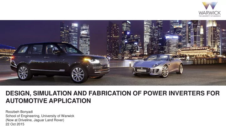
DESIGN, SIMULATION AND FABRICATION OF POWER INVERTERS FOR AUTOMOTIVE APPLICATION Roozbeh Bonyadi School of Engineering, University of Warwick (Now at Driveline, Jaguar Land Rover) 22 Oct 2015 OUTLINE Introduction to power inverters used
DESIGN, SIMULATION AND FABRICATION OF POWER INVERTERS FOR AUTOMOTIVE APPLICATION Roozbeh Bonyadi School of Engineering, University of Warwick (Now at Driveline, Jaguar Land Rover) 22 Oct 2015
OUTLINE • Introduction to power inverters used in automotive • Modelling an automotive power inverter • Design challenges • Fabrication process • Testing the drive cycle • Opportunities • Conclusion 2
INTRODUCTION TO AUTOMOTIVE POWER INVERTER • Converts DC power of the battery to AC power for e-Machine. • Active components • IGBTs or MOSFETs Battery Pack • PiN diodes or Schottky diodes ICE • Passive components • DC-link capacitors • Filters High Power Automotive Cables Power Inverter • Driver board and controller E-Machine 3
POWER ELECTRONICS IN TRACTION DRIVE SYSTEM • The goal is to reduce cost, weight and volume and increase the efficiency. Power Electronics Year ($/kW) (kW/kg) (kW/l) Efficiency 2010 7.9 10.8 8.7 >90% 2012 7 11.2 10 >91% 2015 5 12 12 >93% 2020 3.3 14 13.4 >94% 4
EXAMPLES OF EV AND PHEV ~17 Miles on electric range ~75 Miles on electric range ~250 Miles on electric range 60 kW electric drive 80 kW electric drive 270 kW electric drive 5
POWER INVERTER Toyota Prius Inverter Nissan Leaf Inverter Tesla Model S Inverter (single phase) Electroless Plated Surface Al Wire Bond Solder Die Copper Ceramic Copper 6 Electroless Plated Surface
CONTEXT AND RELEVANCE – Rapid and frequent temperature change is the main cause of power inverter failure! Driving Uphill : Higher Torque → Higher Motor Current → Higher Power Dissipation → Higher Device Temperature Driving Downhill : Lower Torque → Lower Motor Current → Lower Power Dissipation → Lower Device Temperature Driving Fast : Higher Torque and Speed → Higher Motor Current → Higher Power Dissipation → Higher Device Temperature Driving Slow : Lower Torque and Speed → Lower Motor Current → Lower Power Dissipation → Lower Device Temperature Electro-thermal modelling of power electronic system is important during the design phase 7
MODELLING POWER ELECTRONIC DEVICES – IGBT Model Reconstruct Ambipolar Diffusion Equation 8
MODELLING POWER ELECTRONIC DEVICES – Diode Model z Reverse Recovery y Electrons P+ N- N+ P + N - N + x Charge Extraction Charge Extraction 9
MODELLING POWER ELECTRONIC SYSTEM – Electrothermal Modelling Block Diagram Diode and IGBT junction temperature Heatsink temperature during a drive Conduction & Switching Losses Experiments cycle Look Up Table (LUT) (1) Simulink Phase current Waveforms Losses LUT (2) Select Physical Device Motor speed/torque profile Post Simulation From Model (1) or Initial Inductive Switching Test Rig Design an appropriate heatsink (2) Slow, Accurate, Simulation – Thermal resistance Complex Outputs – Thermal capacitance Parameter 1. Diode, IGBT/MOSFET Junction Temperature Extraction 2. Heatsink Temperature PSIM 3. Phase Current 4. Motor Speed/Torque Power Converter System profile Conduction & Switching Electro-Thermal Model 5. Appropriate Heatsink Losses LUT from the Thermal Resistance and Simulator or Experiments Capacitance Fast, Ideal Switching, Simple Models 10
PARASITIC INDUCTANCE MODELLING – Comsol multiphysics Bot Collector Bot Emitter Top Emitter Gate Top Collector 11
PARASITIC INDUCTANCE CALCULATION – Comsol multiphysics Resistance (m Ω ) Inductance (nH) Bottom Switch Collector 10.4381 0.358294 Bottom Switch Emitter 0.906044 0.0214592 Gate 2.53047 0.0817967 Top Switch Collector 1.10261 0.0267436 Top Switch Emitter 3.11811 0.087062 Wirebond (per wire) 5.91523 5.78 12
POWER INVERTER PACKAGING – University of Warwick Packaging Facilities 13
POWER INVERTER PROTOTYPING V.1 14
SWITCHING CHARACTERISTIC – Clamped Inductive Switching Test rig IGBT Turn-on IGBT Turn-off 15
POWER INVERTER PROTOTYPING V.2 – Double side cooling IGBT and diodes, Wire bond-less • CooliR 2 IGBT Dies • Flip die and die up device configurations • Achieve the lowest inductance and shortest current loop • Double side cooling • Wire bond-less module • Flip die (FD) Higher reliability • Higher power density Die up (DU) 16
POWER INVERTER PROTOTYPING V.2 – Double side cooling IGBT and diodes, Wire bond-less 58.6 mm • Three phase inverter • Almost the same size as iPhone 4 (the small one) • Sandwiched dies between two AlN DBC layers 115.2 mm iPhone 4
POWER INVERTER PROTOTYPING V.2 – Double side cooling IGBT and diodes, Wire bond-less • AlSiC top and bottom side pinfin cooling • High thermal conductivity • CTE close to other layers • Higher reliability
OPPORTUNITIES – Future of Automotive Power Inverters By 2020 19
THANK YOU! – Any questions? “ It's about creating the next generation of power devices that are more efficient at using electricity and do so with less heat loss… This is the next generation of semiconductors to replace the silicon chip… The country that figures out how to do this first, and the companies that figure out how to do this best, they're going to be the ones that attract the jobs that go with them.” President Obama, North Carolina, January 2014 20
Recommend
More recommend
Explore More Topics
Stay informed with curated content and fresh updates.

