Array-Based Architecture for Molecular Electronics Andr DeHon - PDF document
Array-Based Architecture for Molecular Electronics Andr DeHon <andre@cs.caltech.edu> DeHon February 2002 Molecular Scale Building Blocks Chemists starting to demonstrate Molecular-scale switching devices Molecular-scale
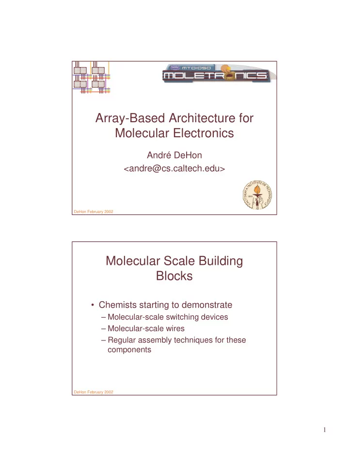
Array-Based Architecture for Molecular Electronics André DeHon <andre@cs.caltech.edu> DeHon February 2002 Molecular Scale Building Blocks • Chemists starting to demonstrate – Molecular-scale switching devices – Molecular-scale wires – Regular assembly techniques for these components DeHon February 2002 1
Computing? • Problem: How can we build computing devices from this technology? – Organize into useful connectivity? – Provide signal restoration? – Personalize/Engineer to perform specific computation? – Accommodate defects? DeHon February 2002 Architecture Goal • This talk: – Starting with these building blocks – Show how to build universal, programmable computing array. DeHon February 2002 2
Outline • Review Components • Restoring Logic Style • Bootstrap Programming • Routing • Defect Tolerance • Summary DeHon February 2002 Wires SiNW (Silicon SWNT (Single Wall Nanowires) Carbon Nanotubes) • Dope to control electrical properties • Nanometer(s) diameter • microns long • good conductors DeHon February 2002 3
Devices Electrostatic Diode and FET Junctions Switches DeHon February 2002 Unique Characteristics • Can only build very regular structures at nanoscale – Arrays of crossed tubes / wires • Will have many defects • Can store state of switch in wire crossing – Contrast with VLSI where switch >> wire xing • Switching occurs at tube/wire crossing – Not at substrate…long term 3D opportunity DeHon February 2002 4
Strategy DeHon February 2002 Strategy • Arrays of FETs for gain • FET decode for bootstrap program • PLA logic in arrays • Overlapping wires for interconnect DeHon February 2002 5
Logic Discipline DeHon February 2002 Diode Logic • Arise directly from touching NW/NTs • Passive logic • Non-restoring DeHon February 2002 6
PMOS-like Restoring FET Logic • Use FET connections to build restoring gates • Static load – Like NMOS (PMOS) DeHon February 2002 PMOS-like Logic DeHon February 2002 7
Operating Point DeHon February 2002 Programmed FET Arrays DeHon February 2002 8
Interfacing and Programming Micro → nanoscale DeHon February 2002 FET Decoders • FETs also ideal for decoding/drive at nano-micro interface DeHon February 2002 9
Program Decoder • Will need to program the decoder – Different scheme; in fabrication – Imprinting/stamping DeHon February 2002 Operating Array • Decoders allow program array – OR, NOR • Isolatable • Dual role of loads during operation • Output used directly by consumer DeHon February 2002 10
Assembly • Overlapping NW/NT between arrays provide interconnect • NOR only sufficient • Alternate: – Programmable (non-restoring) OR – followed by fixed (restoring) NOR DeHon February 2002 Routing • X-Y, mesh routing with appropriate tile overlap DeHon February 2002 11
Defect Tolerance All components (PLA, routing) interchangeable; Allows local programming around faults DeHon February 2002 Summary • Universal, Programmable Architecture – Built entirely from large arrays of crossed NT/NWs • Provides restoration and inversion entirely at nanoscale • Support nanoscale bootstrap programming • Designed to tolerate defective components DeHon February 2002 12
Recommend
More recommend
Explore More Topics
Stay informed with curated content and fresh updates.
![Cache Performance 1 C and cache misses (1) int array[1024]; // 4KB array int even_sum = 0,](https://c.sambuz.com/862609/cache-performance-s.webp)
