Architecture of 80386 The Internal Architecture of 80386 is - PowerPoint PPT Presentation
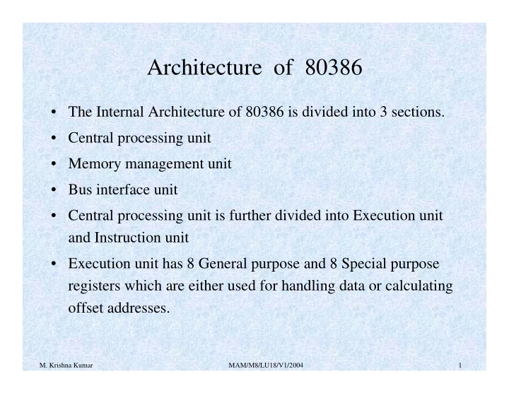
Architecture of 80386 The Internal Architecture of 80386 is divided into 3 sections. Central processing unit Memory management unit Bus interface unit Central processing unit is further divided into Execution unit and
Architecture of 80386 • The Internal Architecture of 80386 is divided into 3 sections. • Central processing unit • Memory management unit • Bus interface unit • Central processing unit is further divided into Execution unit and Instruction unit • Execution unit has 8 General purpose and 8 Special purpose registers which are either used for handling data or calculating offset addresses. M. Krishna Kumar MAM/M8/LU18/V1/2004 1
Architecture of 80386 (cont..) M. Krishna Kumar MAM/M8/LU18/V1/2004 2
Architecture of 80386 (cont..) • The Instruction unit decodes the opcode bytes received from the 16-byte instruction code queue and arranges them in a 3- instruction decoded instruction queue. • After decoding them pass it to the control section for deriving the necessary control signals. The barrel shifter increases the speed of all shift and rotate operations. • The multiply / divide logic implements the bit-shift-rotate algorithms to complete the operations in minimum time. • Even 32- bit multiplications can be executed within one microsecond by the multiply / divide logic. M. Krishna Kumar MAM/M8/LU18/V1/2004 3
Architecture of 80386 (cont..) • The Memory management unit consists of a Segmentation unit and a Paging unit. • Segmentation unit allows the use of two address components, viz. segment and offset for relocability and sharing of code and data. • Segmentation unit allows segments of size 4Gbytes at max. • The Paging unit organizes the physical memory in terms of pages of 4kbytes size each. • Paging unit works under the control of the segmentation unit, i.e. each segment is further divided into pages. The virtual memory is also organizes in terms of segments and pages by the memory management unit. M. Krishna Kumar MAM/M8/LU18/V1/2004 4
Architecture of 80386 (cont..) • The Segmentation unit provides a 4 level protection mechanism for protecting and isolating the system code and data from those of the application program. • Paging unit converts linear addresses into physical addresses. • The control and attribute PLA checks the privileges at the page level. Each of the pages maintains the paging information of the task. The limit and attribute PLA checks segment limits and attributes at segment level to avoid invalid accesses to code and data in the memory segments. M. Krishna Kumar MAM/M8/LU18/V1/2004 5
Architecture of 80386. • The Bus control unit has a prioritizer to resolve the priority of the various bus requests. • This controls the access of the bus. The address driver drives the bus enable and address signal A 0 – A 31. The pipeline and dynamic bus sizing unit handle the related control signals. • The data buffers interface the internal data bus with the system bus. M. Krishna Kumar MAM/M8/LU18/V1/2004 6
Signal Descriptions of 80386 (cont..) • CLK 2 :The input pin provides the basic system clock timing for the operation of 80386. • D 0 – D 31 :These 32 lines act as bidirectional data bus during different access cycles. • A 31 – A 2 : These are upper 30 bit of the 32- bit address bus. • BE 0 to BE 3 : The 32- bit data bus supported by 80386 and the memory system of 80386 can be viewed as a 4- byte wide memory access mechanism. The 4 byte enable lines BE 0 to BE 3 , may be used for enabling these 4 blanks. Using these 4 enable signal lines, the CPU may transfer 1 byte / 2 / 3 / 4 byte of data simultaneously. M. Krishna Kumar MAM/M8/LU18/V1/2004 7
Signal Descriptions of 80386 (cont..) Pin Diagram Of 80386 M. Krishna Kumar MAM/M8/LU18/V1/2004 8
Signal Descriptions of 80386 (cont..) Pin diagram M. Krishna Kumar MAM/M8/LU18/V1/2004 9
Signal Descriptions of 80386 (cont..) CLK 2 ADDRESS A2– A 31 2X CLOCK BUS BE 3# 32 BIT DATA DATA BE 2# D0– D 31 32 – BIT BUS BYTE ADDRESS BE 1# ENABLI NES BE 0# ADS # W / R # NA # D / C# BS16 # M / IO BUS CYCLE BUS DEFINATION CONTROL READY 80386 LOCK # PROCESSOR HOLD PEREQ BUS COPROCESS HLDA BUSY # ARBITRATION OR SIGNALLING ERROR # INTR VCC NMI POWER INTERRUPTS CONNECTIO GND NS RESET Fig: M. Krishna Kumar MAM/M8/LU18/V1/2004 10
Signal Descriptions of 80386 (cont..) • W/R#: The write / read output distinguishes the write and read cycles from one another. • D/C#: This data / control output pin distinguishes between a data transfer cycle from a machine control cycle like interrupt acknowledge. • M/IO#: This output pin differentiates between the memory and I/O cycles. • LOCK#: The LOCK# output pin enables the CPU to prevent the other bus masters from gaining the control of the system bus. • NA#: The next address input pin, if activated, allows address pipelining, during 80386 bus cycles. M. Krishna Kumar MAM/M8/LU18/V1/2004 11
Signal Descriptions of 80386 (cont..) • ADS#: The address status output pin indicates that the address bus and bus cycle definition pins( W/R#, D/C#, M/IO#, BE 0 # to BE 3 # ) are carrying the respective valid signals. The 80383 does not have any ALE signals and so this signals may be used for latching the address to external latches. • READY#: The ready signals indicates to the CPU that the previous bus cycle has been terminated and the bus is ready for the next cycle. The signal is used to insert WAIT states in a bus cycle and is useful for interfacing of slow devices with CPU. • VCC : These are system power supply lines. • VSS : These return lines for the power supply. M. Krishna Kumar MAM/M8/LU18/V1/2004 12
Signal Descriptions of 80386 ( cont..) • BS 16 #: The bus size – 16 input pin allows the interfacing of 16 bit devices with the 32 bit wide 80386 data bus. Successive 16 bit bus cycles may be executed to read a 32 bit data from a peripheral. • HOLD : The bus hold input pin enables the other bus masters to gain control of the system bus if it is asserted. • HLDA : The bus hold acknowledge output indicates that a valid bus hold request has been received and the bus has been relinquished by the CPU. • BUSY#: The busy input signal indicates to the CPU that the coprocessor is busy with the allocated task. M. Krishna Kumar MAM/M8/LU18/V1/2004 13
Signal Descriptions of 80386 (cont…) • ERROR#: The error input pin indicates to the CPU that the coprocessor has encountered an error while executing its instruction. • PEREQ : The processor extension request output signal indicates to the CPU to fetch a data word for the coprocessor. • INTR : This interrupt pin is a maskable interrupt, that can be masked using the IF of the flag register. • NMI: A valid request signal at the non-maskable interrupt request input pin internally generates a non- maskable interrupt of type2. M. Krishna Kumar MAM/M8/LU18/V1/2004 14
Signal Descriptions of 80386. • RESET : A high at this input pin suspends the current operation and restart the execution from the starting location. • N / C : No connection pins are expected to be left open while connecting the 80386 in the circuit. M. Krishna Kumar MAM/M8/LU18/V1/2004 15
Register Organisation (cont..) • The 80386 has eight 32 - bit general purpose registers which may be used as either 8 bit or 16 bit registers. • A 32 - bit register known as an extended register, is represented by the register name with prefix E. • Example : A 32 bit register corresponding to AX is EAX, similarly BX is EBX etc. • The 16 bit registers BP, SP, SI and DI in 8086 are now available with their extended size of 32 bit and are names as EBP,ESP,ESI and EDI. • AX represents the lower 16 bit of the 32 bit register EAX. • BP, SP, SI, DI represents the lower 16 bit of their 32 bit counterparts, and can be used as independent 16 bit registers. M. Krishna Kumar MAM/M8/LU18/V1/2004 16
Register Organisation (cont..) GENERAL DATA AND ADDRESS REGISTERS 31 16 15 0 AX EAX BX EBX CX ECX DX EDX SI ESI EDI DI EBP BP ESP SP SEGMENT SELECTOR REGISTERS CS CODE SEGMENT SS STACK SEGMENT DS DATA SEGMENT ES FS GS INSTRUCTION POINTER AND FLAG REGISTER 31 16 15 0 IP EIP FLAGS EFLAGS Fig: M. Krishna Kumar MAM/M8/LU18/V1/2004 17
Register Organisation (cont..) • The six segment registers available in 80386 are CS, SS, DS, ES, FS and GS. • The CS and SS are the code and the stack segment registers respectively, while DS, ES, FS, GS are 4 data segment registers. • A 16 bit instruction pointer IP is available along with 32 bit counterpart EIP. • Flag Register of 80386 : The Flag register of 80386 is a 32 bit register. Out of the 32 bits, Intel has reserved bits D 18 to D 31 , D 5 and D 3 , while D 1 is always set at 1.Two extra new flags are added to the 80286 flag to derive the flag register of 80386. They are VM and RF flags. M. Krishna Kumar MAM/M8/LU18/V1/2004 18
Register Organisation (cont..) FLAGS 31 18 17 16 15 14 13 12 11 10 9 8 7 6 5 4 3 2 1 0 F L 1 CF RESERVED FOR VM RF 0 NT IOPL OF DF IF TF SF ZF 0 AF 0 PF A INTEL G S FLAG REGISTER OF 80386 M. Krishna Kumar MAM/M8/LU18/V1/2004 19
Recommend
More recommend
Explore More Topics
Stay informed with curated content and fresh updates.
