Allpix > Athena Student Instrumentation Weekly Update March 18th - PowerPoint PPT Presentation
18/03/16 Meng, Ben Nachman, Veronica Wallangen Mathieu Benoit, Philippe Grenier, Lingxin Allpix > Athena Student Instrumentation Weekly Update March 18th Rebecca Carney 1 Overview RMD Carney 18/03/16 Allpix radiation damage
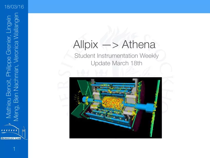
18/03/16 Meng, Ben Nachman, Veronica Wallangen Mathieu Benoit, Philippe Grenier, Lingxin Allpix —> Athena Student Instrumentation Weekly Update March 18th Rebecca Carney 1
Overview RMD Carney 18/03/16 Allpix radiation damage digitizer migration ATLAS Reconstruction chain Digitization: step-by-step Digitization: radiation damage considerations PixelDigitization in Athena Next steps 2
Atlas Reconstruction Chain RMD Carney 18/03/16 From physics events to detector hits Generation to reconstructed interactions HepMC Simulation Event generation G4 MonteCarlo G4 Hits Digitization Digitization Atlfast G4 Digits Reconstruction Real Data ESD Create AOD AOD Analysis 3 Track reconstruction
Digitization step RMD Carney 18/03/16 Ionising interactions liberate Create an analog signal, add noise, free charge carriers in the depleted bulk of the material. The bias across the device creates an electric field which the charge carriers move within, holes in one create digit direction, electrons in the other. This movement within the bulk induces a current on the collecting electrodes. This current continues until the free charge carriers recombine at their respective electrodes. Before the digitizer ‘digitizes’ it must create an analog signal in the detector based on the particle type, energy, and path length within the detector volume. 4
Pixel digitizer: step-by-step RMD Carney 18/03/16 Step 1: Segment path The basic setup is the same for both the current and new charge() functions: energy deposited over the entire path length of the particle’s trajectory is divided up into equal segments. 5
Pixel digitizer: step-by-step RMD Carney 18/03/16 Step 2: Segment charge created / energy deposited in each step For each step along the path, segment the energy deposited into a finite number of chunks (~50 per step by default). + - + - + - + - + - + - + - + - + - + - + - + - + - + - + - + - + - + - + - + - 6
Pixel digitizer: step-by-step RMD Carney 18/03/16 Step 3: di ff use charge in plane + - . . The charges are diffused parallel to the electrode (i.e. in x and y) and in one of those directions (assuming a given orientation) the charges will also get a contribution from 7 the Lorentz force.
Pixel digitizer: step-by-step RMD Carney 18/03/16 Step 4: drift charge in E-field to electrode + - If no charge is trapped the induced signal on the electrode integrated in time is equal to the total charge recombining at the electrode: so the original digitizer just drifts the charge parallel to the electrode and establishes the pixel where that charge would be collected, then passes it to the 8 digitizing portion of the code.
slide title RMD Carney 18/03/16 Subtitle 9
Rad damage: step-by-step RMD Carney 18/03/16 Step 5: Trapping and LUTs 1. From the electric field at the charge carrier’s starting depth and the mobility of the charge carrier: the time-to-electrode is looked up (LUT). 2. The drift time of this particular charge chunk is also calculated - this involves the probability that the charge will be trapped and is dependent on fluence. 3. If the drift time < time-to-electrode, the charge is trapped. 4. The depth at which the carrier is trapped is checked in a LUT. 5. The Weighting (Ramo) potential for the initial position (creation) and final (trapped) position of the charge carrier is checked in a LUT. 6. And hence the induced signal up to the point of trapping is calculated and added to the chargedDiodes collection. 10 7. The effect of moving charge carriers on neighboring pixels (i.e. charge sharing) is also provided from an LUT.
Ramo (weighting field)?? RMD Carney 18/03/16 What did we assume? How is this better? First, some key points 1. The Electric field determines the charge trajectory and velocity. Neither of these have anything to do with the weighting field, so if you want to know them at a particular point you must go through the entire process using Gauss’s law, etc. 2. The weighting field depends only on the geometry of the electrodes and determines how the charge’s motion couples to a specific electrode to induce a signal. 3. Only in 2-electrode configurations are the weighting field and Electric field the same shape (and they are still only proportional not identical)![2] The weighting field for smaller electrodes is weird So, that’s what this picture is! It’s the weighting field for a pixel. It’s interesting because it shows that the majority of contribution to the signal is localized directly under the pixel. Weighting potential: A single pixel 11 Weighting potential: 2 ∞ -planar electrodes Weighting potential: ∞ strip
Pixel digitizer: step-by-step RMD Carney 18/03/16 Subtitle 1. From the electric field at the charge carrier’s starting depth and the mobility of the charge carrier: the time-to-electrode is looked up (LUT). 2. The drift time of this particular charge chunk is also calculated - this involves the probability that the charge will be trapped and is dependent on fluence. 3. If the drift time < time-to-electrode, the charge is trapped. 4. The depth at which the carrier is trapped is checked in a LUT. 5. The Weighting (Ramo) potential for the initial position (creation) and final (trapped) position of the charge carrier is checked in a LUT. 6. And hence the induced signal up to the point of trapping is calculated and added to the chargedDiodes collection. 7. The effect of moving charge carriers on neighboring pixels (i.e. charge sharing) is also 12 provided from an LUT.
Pixel digitizer: step-by-step RMD Carney 18/03/16 Step 5: Induced charge contribution 1. From the electric field at the charge carrier’s starting depth and the mobility of the charge carrier: the time-to-electrode is looked up (LUT). 2. The drift time of this particular charge chunk is also calculated - this involves the probability that the charge will be trapped and is dependent on fluence. 3. If the drift time < time-to-electrode, the charge is trapped. 4. The depth at which the carrier is trapped is checked in a LUT. 5. The Weighting (Ramo) potential for the initial position (creation) and final (trapped) position of the charge carrier is checked in a LUT. 6. And hence the induced signal up to the point of trapping is calculated and added to the chargedDiodes collection. 7. The effect of moving charge carriers on neighboring pixels (i.e. charge sharing) is also 13 provided from an LUT.
Pixel Digitization: workflow RMD Carney 18/03/16 Rough (relevant) workflow: Pixel digitization In PDT::initialize(), all of the tools and services are linked and added by ‘StoreTool()’ and ‘retrieve()’ and then an ‘add’ function that calls the process() method in each tool. Only SurfaceChargeTools does not get added at this stage. The <Technology> is the specific element type, e.g. PixelECChargeTool, Ibl3DChargeTool, etc. Each of these classes contain a ‘charge()’ method that adds diffusion, propagates the charge in steps, and adds sensor efficiency maps (if necessary). applyProcessorTools() calls the various services that add to the signal (noise, ‘smearing’), and also pass the analog signal through a discriminator. The PDT::createRDO method is where mask/sub-threshold/disabled-element/corrupted flags are applied and where ToT is calculated via a call to CalibSvc. PixelDigitization PixelDigitizationTool::processAllSubEvents() (PDT)::digitizeAllHits() (PDT)::digitizeNonHits() (PDT)::applyProcessorTools() (PDT)::createAndStoreRDO() (PDT)::digitizeElement() (PDT)::createRDO() SurfaceChargeTools::process() 14 <Technology>::charge()
Pixel digitizer: tools in Athena RMD Carney 29/02/16 applyProcessorTools() calls an instance of each derived class of ISiChargedDiodesProcessorTool interface: all of which are the discriminator/noise/crosstalk tools! Athena structure A service serves many clients, a tool only one. A service typically has one instance but a tool may have many. It is appropriate that we use a tool for this work. 15
RadDamage Tools RMD Carney 18/03/16 Introduction The Allpix team have produced a standalone test bench for, among other things, a Additional charge tool and utility digitizer that models the effects of radiation damage in Silicon: notably by considering the effects of trapping and partial signal loss that comes with it, as well as charge sharing. I’ve been tasked with migrating the relevant parts of that digitizer into Athena. class IblPlanarRadDamageTool : SubChargesTool Two classes added to: InnerDetector/InDetDigitization/ Creates the analog signal using overloaded charge() PixelDigitization/ method from base class. Format is almost identical to equivalent unirradiated uniform & Bichsel versions but includes some checks for trapping. This first draft only includes a class for the IBL planar modules but it seems feasible (given that the classes are near identical) that I can produce class RadDamageUtil : AthAlgTool the equivalent for the Pixel Barrel/EC as well. A collection of function used to calculate the radiation damage effects and process trapping/induced current. The IBL 3D models in Allpix are not Like Bichsel, a separate tool is needed as these yet ready but are a tiny fraction of the calculations are independent of sensor geometry and detector anyway. conditions - parameters can be fed in as arguments (e.g. pointer to Ramo weighting map and sensor bias). 16
Recommend
More recommend
Explore More Topics
Stay informed with curated content and fresh updates.
