A 45 W Bias Power, 34 dB Gain Reflection Amplifier Exploiting the - PowerPoint PPT Presentation
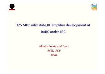
A 45 W Bias Power, 34 dB Gain Reflection Amplifier Exploiting the Tunneling Effect for RFID Applications Francesco Amato, Christopher W. Peterson, Brian D. Degnan, Gregory D. Durgin School of Electrical and Computer Engineering Georgia
A 45 μ W Bias Power, 34 dB Gain Reflection Amplifier Exploiting the Tunneling Effect for RFID Applications Francesco Amato, Christopher W. Peterson, Brian D. Degnan, Gregory D. Durgin School of Electrical and Computer Engineering Georgia Institute of Technology
Reflection amplifiers 1 2 > 1 M = 0.25 M = 1 M > 1 Reflection amplifiers are active devices that, when opportunity biased, display a negative resistance (-R).
Power consumption Dalman72 Chan2011 Cantu2006 Cantu2008 Chan2013 Lazaro2013 Kimionis2014
Quantum tunneling Tunnel Diode IV curve Tunnel Diode IV curve 0.6 0.5 0.4 0.3 0.2 I [mA] 0.1 I [mA] 0 -0.1 -0.2 > 1 -0.3 -0.4 -0.5 -0.6 -0.05 0 0.05 0.1 0.15 0.2 0.25 0.3 0.35 0.4 0.45 V [V] V [V]
The design Aeroflex Metelics MBD5057-E28 Tunnel diode equivalent circuit
The design Schematic Microstrip model
Reflection Amplifier Characterization (1/2) • How does it behave at different input frequencies? • What happens to amplitude and phase of the reflected RF signals? Vector • VNA E5071B Analyzer • Avg on 16 traces • RF P in = -50 dBm
Reflection Amplifier Characterization (1/2) Vector Analyzer • Optimum bias voltage: 80 mV • Measured current: 566 μ A • P bias = 45.28 μ W
Reflection Amplifier Characterization (1/2) Vector Analyzer • Optimum bias voltage: 90 mV • Measured current: 525 μ A • P bias = 47.25 μ W
Reflection Amplifier Characterization (1/2) Vector Analyzer • Δφ 1 = 45 ˚ • Δφ 2 = 53 ˚
Reflection Amplifier Characterization (2/2) • At what RF input power levels is the gain available? • What is the bandwidth of the reflection amplifier? • How does the gain change with bias voltages? Reflection Amplifier • Sig. Gen. E8247C • Sig. An. CXA-N9000A Signal • Res BW: 3 kHz Generator • Video BW: 100 kHz • Span: 1 MHz • Avg: 10 Signal • Points: 1001 Attenuators Analyzer
Reflection Amplifier Characterization (2/2) Reflection Amplifier Signal Generator Signal Analyzer • Used bias powers: 45 μW and 47 μW • Max gains: 34.4 dB and 22.1 dB • Input frequencies: 5.45 GHz, 5.55 GHz
Reflection Amplifier Characterization (2/2) Reflection Amplifier Signal Generator Signal Analyzer • Used bias voltages: 80 and 90 mV • Input powers: -70 dBm and -60 dBm
Reflection Amplifier Characterization (2/2) Reflection Amplifier Signal Generator Signal Analyzer • Input frequencies: 5.45 GHz and 5.55 GHz • Input powers: -70 dBm and -60 dBm
Modulated spectrum -20 Backscattering from semi passive tag Backscattering from reflection amplifier with tunnel diode -30 -40 Modulation with 250 kHz square wave Input RF power: -60 dBm -50 P out [dBm] 35.6 dB gain -60 -70 -80 -90 -100 5.7997 5.7998 5.7999 5.8 5.8001 5.8002 5.8003 Frequency [GHz]
Conclusions • High reflection gains achieved with Dalman72 low power consumptions Cantu2006 Chan2011 • Working with RF input powers Cantu2008 Chan2013 Kimionis2014 as low as -90 dBm Lazaro2013 -20 Backscattering from semi passive tag Backscattering from reflection amplifier with tunnel diode -30 -40 -50 P out [dBm] -60 -70 -80 -90 -100 5.7997 5.7998 5.7999 5.8 5.8001 5.8002 5.8003 Frequency [GHz] Thank you f.amato@gatech.edu
Backscatter Modulation
Power consumption
Degenerate Semiconductors Tunnel Diode When a p-n junction is formed, a Semiconductors heavily doped with thin junction region is created as donors (n-type) have the Fermi result of keeping the continuity of level up inside the conduction band the Fermi level Semiconductors heavily doped with acceptors (p-type), have the Fermi level inside the valence band I This results in a finite probability that electrons overcome the energy barrier when a small V biasing voltage is applied ( quantum tunneling [3])
Semiconductors I V Energy band diagram, diode
Recommend
More recommend
Explore More Topics
Stay informed with curated content and fresh updates.

