9 STIS On-Orbit Detector Performance Figure 1. Quantum Efficiency - PDF document
1997 HST Calibration Workshop Space Telescope Science Institute, 1997 S. Casertano, et al., eds. The On-Orbit Performance of the STIS Detectors 1 Randy A. Kimble 2 Laboratory for Astronomy and Solar Physics, Goddard Space Flight Center,
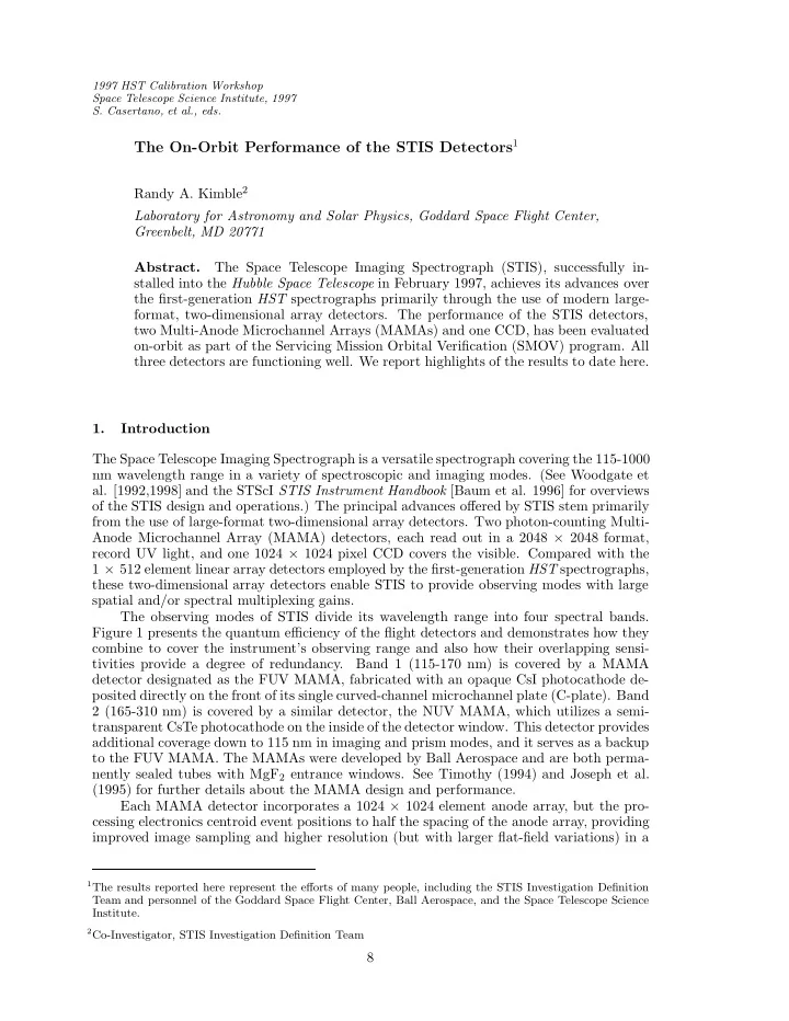
1997 HST Calibration Workshop Space Telescope Science Institute, 1997 S. Casertano, et al., eds. The On-Orbit Performance of the STIS Detectors 1 Randy A. Kimble 2 Laboratory for Astronomy and Solar Physics, Goddard Space Flight Center, Greenbelt, MD 20771 The Space Telescope Imaging Spectrograph (STIS), successfully in- Abstract. stalled into the Hubble Space Telescope in February 1997, achieves its advances over the first-generation HST spectrographs primarily through the use of modern large- format, two-dimensional array detectors. The performance of the STIS detectors, two Multi-Anode Microchannel Arrays (MAMAs) and one CCD, has been evaluated on-orbit as part of the Servicing Mission Orbital Verification (SMOV) program. All three detectors are functioning well. We report highlights of the results to date here. 1. Introduction The Space Telescope Imaging Spectrograph is a versatile spectrograph covering the 115-1000 nm wavelength range in a variety of spectroscopic and imaging modes. (See Woodgate et al. [1992,1998] and the STScI STIS Instrument Handbook [Baum et al. 1996] for overviews of the STIS design and operations.) The principal advances offered by STIS stem primarily from the use of large-format two-dimensional array detectors. Two photon-counting Multi- Anode Microchannel Array (MAMA) detectors, each read out in a 2048 × 2048 format, record UV light, and one 1024 × 1024 pixel CCD covers the visible. Compared with the 1 × 512 element linear array detectors employed by the first-generation HST spectrographs, these two-dimensional array detectors enable STIS to provide observing modes with large spatial and/or spectral multiplexing gains. The observing modes of STIS divide its wavelength range into four spectral bands. Figure 1 presents the quantum efficiency of the flight detectors and demonstrates how they combine to cover the instrument’s observing range and also how their overlapping sensi- tivities provide a degree of redundancy. Band 1 (115-170 nm) is covered by a MAMA detector designated as the FUV MAMA, fabricated with an opaque CsI photocathode de- posited directly on the front of its single curved-channel microchannel plate (C-plate). Band 2 (165-310 nm) is covered by a similar detector, the NUV MAMA, which utilizes a semi- transparent CsTe photocathode on the inside of the detector window. This detector provides additional coverage down to 115 nm in imaging and prism modes, and it serves as a backup to the FUV MAMA. The MAMAs were developed by Ball Aerospace and are both perma- nently sealed tubes with MgF 2 entrance windows. See Timothy (1994) and Joseph et al. (1995) for further details about the MAMA design and performance. Each MAMA detector incorporates a 1024 × 1024 element anode array, but the pro- cessing electronics centroid event positions to half the spacing of the anode array, providing improved image sampling and higher resolution (but with larger flat-field variations) in a 1 The results reported here represent the efforts of many people, including the STIS Investigation Definition Team and personnel of the Goddard Space Flight Center, Ball Aerospace, and the Space Telescope Science Institute. 2 Co-Investigator, STIS Investigation Definition Team 8
9 STIS On-Orbit Detector Performance Figure 1. Quantum Efficiency of the STIS Flight Detectors 2048 × 2048 image format (Kasle & Morgan 1991). For historical reasons, this is referred to as the high resolution mode; all generic references to MAMA pixels in this paper (and in most other STIS documentation) refer instead to low-resolution pixels in the 1024 × 1024 format. Bands 3 and 4 (305-555 nm; 550-1000 nm) are covered by a backside-thinned, UV- enhanced, multi-pinned-phase, 1024 × 1024 pixel CCD developed by Scientific Imaging Technologies (SITe). The CCD also provides backup to the NUV MAMA in the 180-305 nm range. The CCD is cooled to an operating temperature of -83 C using a four-stage thermoelectric cooler (TEC). The CCD and TEC are enclosed within a sealed, evacuated housing whose fused silica window is only slightly cooler than the rest of the instrument, minimizing the condensation of contaminants which could otherwise be deposited directly onto the much colder CCD. See Kimble et al. (1994) for a more comprehensive discussion of the CCD subsystem. Since launch, a variety of performance and characterization tests have been carried out for STIS as part of the Servicing Mission Orbital Verification (SMOV) program. We report here on the highlights of the detector-related aspects of the SMOV program. For critical parameters that have not yet been or can not be measured directly in flight, we also cite relevant results from the pre-flight calibration. 2. CCD Performance The 1024 × 1024 pixel STIS CCD is a backside-illuminated three-phase device, with 21 µ m pixels, multi-pinned-phase implants and operation, and an enhanced UV response. The backside UV-enhancement process was developed by SITe for the STIS program. The resulting quantum efficiency (Figure 1) is stable, does not show QE hysteresis, and does not require a UV flood.
10 Kimble et al. The CCD is fabricated with a readout amplifier in each of the four corners. There is an independent analog signal processing chain for each amplifier, and the STIS flight software supports full-frame, on-chip-binned, or subarray readout with any of the four amplifiers, as well as two and four amplifier readout modes. Initial functional testing on orbit verified that all four amplifier chains were functioning nominally. Observations since that first checkout have been carried out exclusively with the lowest noise amplifier, which was most fully characterized in ground testing. The redundant amplifiers are available as future backups. Four commandable gain settings are available for the CCD. The noise performance measured in flight and the dynamic range for each setting are summarized in Table 1. Rough gain measurements made in flight are consistent with the more precisely determined ground values shown in the table. Two gain settings are recommended for general use: gain=1 for the greatest sensitivity to faint targets and gain=4 for the highest dynamic range and full well. Table 1. CCD Noise/Dynamic Range. Single Frame Nominal Gain Measured Gain Noise (rms) Linear Range Dynamic Range = e/DN e/DN In-flight data At 1% Rolloff Linear Range/Noise 1 0.995 4.0 DN = 4.0 e 33,000 e 8,250 2 2.01 2.7 DN = 5.4 e 86,000 e 16,000 4 4.11 1.7 DN = 7.0 e 144,000 e 20,600 8 8.38 1.3 DN = 10.9 e 144,000 e 13,200 In-flight mean bias levels vary over roughly 10 DN (data numbers in the 16-bit digitized readout) at gain=1 and 3 DN at gain=4 (due to temperature variations in the CCD and processing electronics); however, the shape of the bias frames is constant to < 0.2 DN, so the bias level is well determined by the serial and parallel overscan data read out with each CCD frame. Under logarithmic stretch, some frames, particularly at gain=4, show “herringbone” noise that can be discerned by the eye. This pattern is low amplitude, however, < 1 DN, and does not significantly affect the overall noise statistics in the image. Charge transfer efficiency (CTE) was measured by both x-ray and edge response tech- niques in ground calibration, with parallel CTE results of 0.999994 @ 1620 e (x-ray) and 0.999991 @ 200 e, 0.99996 @ 10 e (edge response). Serial CTE’s are higher. Additional ground calibration tests measured the parallel CTE performance under “sparse field” illu- mination, i.e. as would be encountered when observing the spectrum of a point source or an image of a dilute stellar field with only one or two stars per CCD column. These tests implied a charge loss up to 1.1% from the top of the CCD column to the bottom, for signal levels of 500 e/pixel, operating at the gain=1 voltage settings. For higher signal levels or the gain=4 voltage settings, the derived charge loss across the CCD is lower. The x-ray CTE measurements can not be duplicated in flight, and the sparse field measurements have not yet been. However, edge response measurements (using onboard flat-field lamps for illumination) show no significant changes from ground measurements. The median dark current at the CCD operating temperature of -83 C is only ∼ 0.0015 electrons/pixel/second, or 5-6 electrons/pixel/hour. Unless significant on-chip binning is employed, the noise from the median dark current is thus negligible compared with the read noise of the system. Of much greater significance are the effects of cosmic rays and radiation-induced hot pixels. With regard to these issues, the performance of the STIS CCD is very similar to that of WFPC2. The cosmic ray rate observed on the STIS CCD outside of the South Atlantic Anomaly (SAA) is ∼ 1 event/cm 2 /second. Roughly 30-40 pixels/second are affected at greater than a 20 electron level. Cosmic rays are most effectively removed from science data by specifying CR-SPLIT exposures to obtain multiple images from which cosmic rays can be vetoed.
Recommend
More recommend
Explore More Topics
Stay informed with curated content and fresh updates.



![Figure 1: Team Logo 2 Figure 2: AISC SSBC Event Logo [1] Figure 3: Vertical Load locations [1]](https://c.sambuz.com/492196/figure-1-team-logo-s.webp)
