3D-Printed Detectors and Detector Integration modern manufacturing - PowerPoint PPT Presentation
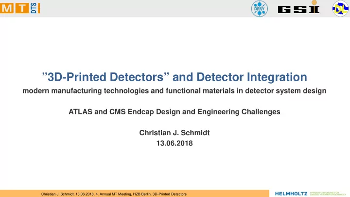
3D-Printed Detectors and Detector Integration modern manufacturing technologies and functional materials in detector system design ATLAS and CMS Endcap Design and Engineering Challenges Christian J. Schmidt 13.06.2018 Christian J.
”3D-Printed Detectors” and Detector Integration modern manufacturing technologies and functional materials in detector system design ATLAS and CMS Endcap Design and Engineering Challenges Christian J. Schmidt 13.06.2018 Christian J. Schmidt, 13.06.2018, 4. Annual MT Meeting, HZB Berlin, 3D-Printed Detectors
Towards 3D-printed Detectors and Detector Integration Functional 3D-printing: Printed particle Detectors from CAD to batch-size 1 production include functionality beyond mechanical shape: Low-Z, low R signal conductors Laser/InkJet-Printed Circuits Complex metallic capillary cooling structures (as e.g. in Belle II upgrade) Semiconductor 3D-post processing (Si/Ge-Det. avoid rad. sensitive surface doping, integration of cooling lines etc.) 3D-printed mechanical structures and interconnect Integration of optical and conductive data interconnect precision field cage degraders The forgotten realm in material thickness (2 to 50µm) precision high purity electrolytic deposition of none copper materials molecular plating of compounds for high purity surfaces realization of low-Z power and signal lines as well as via-connections e.g. Ink-Jet print on 3D-Surfaces, enhance through galvanic build-up
3D-Plastic-Extrusion Printing more and more comonly used 3D-Printing used in detectors and instrumentation for mock-ups and communication David Anderson at DENIM 2015 on the neutron instrument VISION
@ GSI recent heavy use of 3D-Print for ordenary experimental work The CBM-STS developments heavily employ one of 5 Ultimakers Devices rentate in no time Even small series of parts are being printed (~ several hundred) Cheap ~ 5k€ machines serve to provide parts for many applications with little particular demands in material specs. Scientists can easily make their own part and they do! no need to wait weeks for the workshop
Detector Challenges Full 4 π coverage with negligible blind area and high granularity Minimized material budget Active Targets (the target itself enabled as detector) , structured targets Detector power and DAQ Detector power management power distribution cooling GHz data transmission, impedance defined data lines Integration of exotic, active materials Integration of front-end electronics onto Germanium detectors
Beyond Slicing, beyond plastics Example: Hermle Additive Manufacturing Metal powder in a supersonic beam fused to substrate Combination with 5-axis milling center
Extremely lightweight 3D-Cooling Structures low mass in mobile technologies translates to low material budget example motor cylinder head direct cooling translates to electronics power densities direct cooled drills and tools
Technologies rapidly evolving but still mostly island solutions mechanical 3D-printing for shape prototyping functionality beyond shape step by step added electrical conductivity mechanical strength, mechanical bonding strength thermal conductivity material properties (e.g. sensor materials) modern laser structuring tools allow 3D-shaping of dedicated, highly specialized sensor material CdZnTl high Z sensors Diamond Sensors, Diamond membrane sensors, 3D-Diamond Silicon/Germanium sensors ultra low noise detector compounds for astronomy, satellites and astrophysics
Bionic Design Engineering to be learned anew 3D additive manufacturing introduces new dimensions in engineering options Challenge for intellectual exploration Only people can exploit the full potential for future detectors need to let them work and play with new possibilities
Equipment: Technological Directions 3D-Printers, additive manufacturing – ceramic, metallic, plastics.... Conductive ink-jet printers Femtosecond ablation for high aspect ratio micro structures Plasma etching along Bosch-Process Laser Lithography Laser assisted soldering and interconnect LTO (low temperature oxide) capable LPCVD Carbon-Fibre-Composite 3D laying robot
New materials, examples Airex foam with up to 98% air content for rugged sandwich structures Carbon foam Example taped CMS tracker module design, Wim de Boer et al Sinthetic graphite foil heat spreader tape with conductivity like diamond adhesive PET layer assembly and HV isolation conduction lateral little conduction perpendicular to plane
Example: fiber carbon composit structures CBM-STS Beampipe CBM-STS Silicon Detector Ladders
Examples of engineering challenges currently addressed The Phase 2 Upgrades of the ATLAS & CMS Trackers The High-Luminosity LHC • High-luminosity operation will start in 2026 4000 fb -1 expected ultimate integrated luminosity over • ten years • Both ATLAS & CMS will replace their inner tracking detectors The new tracking detectors • Will consist of several thousands of detector modules O(200) m 2 of silicon • • Cooled with evaporative CO 2 and operated below -30 °C
CMS Phase 2 Tracker End Cap Design • Goal is to reduce material budget by a factor of 2 • Backbone is a carbon fibre sandwich half-disk structure • 230 cm in diameter • 10 mm thickness now • Modules are mounted from both sides onto structure < 100 μm positioning precision • • 20 half-disks are combined to build one end cap • 150 cm total length then
CMS Phase 2 Tracker End Cap Design • Six cooling sectors each with ~6 m length • Cooling pipes embedded in • 480 cooling and positioning inserts • 76 carbon foam heat spreaders spanning through the full thickness of the sandwich • Sandwich core is a mixture of structural and carbon foam • 228 additional positioning inserts • Two types of glues used in the same assembly steps • Structural & thermally conductive (boron nitride doped)
CMS Phase 2 Tracker End Cap Design • Cooling and positioning inserts are currently glued onto pipe • Grooves in inserts are closed by lids to increase contact area to pipe • Six cooling sectors each with ~6 m length • What if the insert could be printed • Cooling pipes embedded in around the cooling pipe • 480 cooling and positioning inserts • no adhesive joint ➟ better • 76 carbon foam heat spreaders spanning through the full thickness of the sandwich thermal performance • less assembly work • Sandwich core is a mixture of structural and carbon foam • 228 additional positioning inserts • Two types of glues used in the same assembly steps • Structural & thermally conductive (boron nitride doped)
Prototyping of Support Structures Small Scale Prototype CMS Half-Disk Structure • 35 cm x 40 cm in size • Two cooling loops and corresponding inserts and cooling blocks < 50 μm • Study assembly sequence and precision, and cooling performance Measured offset to nominal insert positions < 65 μm • ATLAS prototype of full-sized petal CAD • 60 cm x 40 cm in size < 65 μm • One cooling loop fully embedded in carbon foam prototype
Thermal Testing The Key to Good Thermal Performance • Understanding of novel raw materials • E.g. thermal impedance between 2.5 mm cooling pipe and carbon foam • Development of machining, handling and processing techniques • Especially if we drive usage beyond the specified regime • Qualification of final support structures • E.g. identify weak thermal contacts via IR thermography
Diagnostics Performance relies on high-quality adhesive bonds • For best mechanical stability and cooling performance • Ultrasonic inspection allows for non-destructive testing • Example: investigation of sandwich structure with carbon fibre facings • 10 mm x 10 mm void in adhesive bond area • uniformity of adhesive bond between carbon foam and facing
Microchannel Cooling Cooling at the Next Level • Conventional cooling relies on thermal conduction between heat source and coolant • Smaller temperature gradient typically means more mass • What if coolant could be brought closer to the heat source? • Ideal for large power densities, e.g. pixel detectors Microchannel cooling: ~100 μm wide • channels etched in silicon substrate • Heat conduction path < 1 mm • Perfect match in terms of coefficient of thermal expansion (CTE) ➟ no thermal stress
One Theme of Distributed Detector Lab: “3D-Printed Detectors” Modern Materials, Modern 3D Structuring Technologies, Modern Additive and Subtractive Machining and Engineering Necessary invest can be financed through the DDL, the brains we need to supply ourselves. • 3D-Printing-oriented Engineering • ultra lightweight structures • combined functionality • power management • complex metallic capillary cooling structures • Integration of optical and conductive data RF carpets to stop interconnect relativistic fragment ions Stopping power ~ Structure 3 SEITE 21
GSI/FAIR Campus Masterplan indicates Area for DDL Infrastructure New lab could find a site: 850 qm real estate Construction limit 23m Could give central home to: Germanium Detector Lab Experiment Electronics ASIC and Si-Pixel Lab Cryo-Detectors Lab 3D-Printing Lab Material Sciences and Nano- Technologies Lab SEITE 22
Recommend
More recommend
Explore More Topics
Stay informed with curated content and fresh updates.
