2. Introduction to Diodes Lecture notes: page 2-1 to 2-19 Sedra - PowerPoint PPT Presentation
2. Introduction to Diodes Lecture notes: page 2-1 to 2-19 Sedra & Smith (6 th Ed): Sec. 3.* and 4.1-4.4 Sedra & Smith (5 th Ed): Sec. 3.7* and Sec. 3.1-3.4 * Includes details of pn junction operation which is not covered in this course
2. Introduction to Diodes Lecture notes: page 2-1 to 2-19 Sedra & Smith (6 th Ed): Sec. 3.* and 4.1-4.4 Sedra & Smith (5 th Ed): Sec. 3.7* and Sec. 3.1-3.4 * Includes details of pn junction operation which is not covered in this course ECE 65, Winter 2013, F. Najmabadi
Energy levels in an atom The larger the energy level, the larger is the spatial extent of electron orbital. Discrete energy levels! Each energy level can be filled with a finite number of electrons. Lowest energy levels are filled first. Nucleus position Electrons in the last filled energy level are called “valance” electrons and are responsible for the chemical properties of the material . F. Najmabadi, ECE 65, Winter2013, Intro to Diodes (2/29)
Energy Bands in Solids Forbidden energy gaps For small inter-distance between energy bands. between ions, energy levels become energy bands. Conduction band : the lowest energy band with electrons NOT tied to the atom. Valance band: the highest energy band with electrons tied to the atom. Band-Gap is the energy difference between the top of valance band and the bottom of conduction band F. Najmabadi, ECE 65, Winter2013, Intro to Diodes (3/29)
Differences among conductors, semiconductors and insulators In a metal, the conduction band is partially filled. These electron can move easily in the material and conduct heat and electricity (Conductors). In a semi-conductor at 0 k the conduction band is empty and valance band is full. o The band-gap is small enough that at room temperature some electrons move to the conduction band and material conduct electricity. An insulator is similar to a semiconductor but with a larger band-gap. Thus, at room temperature very few electrons are in the conduction band. Semiconductor Semiconductor Insulator Metal at T = 0 k at T > 0 k F. Najmabadi, ECE 65, Winter2013, Intro to Diodes (4/29)
Electric current in a semiconductor is due to the motion of electrons and “holes” At T > 0 k, some electrons are promoted Conduction band to the conduction bands. A current flows when electrons in the Valance band conduction band move across the “holes” or available slots material (e.g., due to an applied electric in the valance band field). A current also flows when electrons in the valance band jump between available slots in the valance bands (or “holes”). o An electron moving to the left = a hole moving to the right! o We call this is a “hole” current to differentiate this current due to conduction band electrons. Pure Si Crystal F. Najmabadi, ECE 65, Winter2013, Intro to Diodes (5/29)
Doping increases the number of charge carriers Doped n-type Semiconductor Doped p-type Semiconductor Donor atom (P doping) has an extra Acceptor atom (B doping) has one less electron which is in the conduction band. electrons: a hole in the valance band. Charge Carriers: Charge Carriers: o Electrons due to donor atoms o Holes due to acceptor atoms o Electron-hole pairs due to thermal o Electron-hole pairs due to thermal excitation excitation o e: majority carrier, h: minority carrier o h: majority carrier, e: minority carrier F. Najmabadi, ECE 65, Winter2013, Intro to Diodes (6/29)
Electric current is due to the motion of charge carriers Drift Current: An electric field forces charge carriers to move and establishes a drift current: = µ I drift Aqn E Diffusion Current: As charge carrier move randomly through the material, they diffuse from the location of high concentration to that of a lower concentration, setting up a diffusion current: dn = − | | I diff A q D dx Einstein Relationship: o V T is called the Thermal voltage or D kT = T = V volt-equivalent of temperature µ | | q o V T = 26 mV at room temperature F. Najmabadi, ECE 65, Winter2013, Intro to Diodes (7/29)
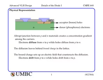
Junction diode Simplified physical structure Construction on a CMOS chip
A pn junction with open terminals (excluding minority carriers) High concentration of h on the p side High concentration of e on the n side Electrons diffuse towards the junction Holes diffuse towards the junction Holes from the p side and electrons from the n side combine at the junction, forming a depletion region I dif I dif n side is positively p side is negatively charged because it charged because it has lost electrons. has lost holes. A potential is formed which inhibits further diffusion of electron and holes (called junction built-in voltage) F. Najmabadi, ECE 65, Winter2013, Intro to Diodes (9/29)
A pn junction with open terminals (including minority carriers) Thermally-generated minority carriers on the n side I dif (holes) move toward the depletion region, and are swept into the p side by the potential where the I S combine with electrons. (similar process for minority carriers on the p side). This sets up a drift current, I S . To preserve charge neutrality, a non-zero I diff = I S should flow (height of potential is slightly lower). I diff scales exponentially with changes in the voltage barrier. I S is independent of the voltage barrier but is a sensitive function of temperature. F. Najmabadi, ECE 65, Winter2013, Intro to Diodes (10/29)
pn Junction with an applied voltage Reverse-Bias: Height of the barrier is increased, reducing I diff I diff approaches zero rapidly, with i D ≈ I S A very small negative i D ! Forward-Bias: Height of the barrier is decreased, increasing I diff I diff increases rapidly with v D leading to i D ≈ I diff A very large positive i D ! F. Najmabadi, ECE 65, Winter2013, Intro to Diodes (11/29)
Diode iv characteristics equation ( ) = − / v D nV 1 i I e T D S I S : Reverse Saturation Current (10 -9 to 10 -18 A) V T : Volt-equivalent temperature (= 26 mV at room temperature) n : Emission coefficient (1 ≤ n ≤ 2 for Si ICs) ≥ For | | 3 v nV D T ≈ / v nV Forward bias : i I e D T D S ≈ − Reverse bias : i I D S Sensitive to temperature: I S doubles for every 7 o C increase V T = T (k) /11,600 For derivation of diode iv equation, see Sedra & Smith Sec. 3 F. Najmabadi, ECE 65, Winter2013, Intro to Diodes (12/29)
Diode Limitations Thermal load , P = i D v D (typically specified as maximum i D ) Reverse Breakdown at Zener voltage ( V Z ) (due to Zener or avalanche effects) Zener diodes are made specially to operate in this region safely! F. Najmabadi, ECE 65, Winter2013, Intro to Diodes (13/29)
How to solve diode circuits?
Diode circuit equations are nonlinear KCL : current in all elements i D = + KVL : v Ri v i D D ( ) = − / v D nV Eq. : 1 iv i I e T D S Two equations in two-unknowns to solve for i D and v D Non-linear equation: cannot be solved analytically Solution methods: o Numerical (PSpice) o Graphical (load-line) o Approximation to get linear equations (diode piece-linear model) F. Najmabadi, ECE 65, Winter2013, Intro to Diodes (15/29)
Graphical Solution (Load Line) KCL : current in all elements i D = + KVL : v Ri v i D D ( ) = − / v D nV Eq. : 1 iv i I e T D S ( ) = − v D nV / 1 i I e T D S Intersection of two curves satisfies both equations v i /R and is the solution i DQ = + v Ri v i D D Load Line v i v DQ F. Najmabadi, ECE 65, Winter2013, Intro to Diodes (16/29)
Diode piecewise-linear model: Diode iv is approximated by two lines Constant Voltage Model Diode ON Diode OFF V D0 Circuit Models: = ≥ Diode ON : and 0 ON: v V i 0 D D D = < Diode OFF : 0 and i v V 0 D D D = − " cut - in" voltage, 0 . 6 0 . 7 V for Si V D 0 OFF: F. Najmabadi, ECE 65, Winter2013, Intro to Diodes (17/29)
Recipe for solving diode circuits (State of diode is unknown before solving the circuit) 1. Write down all circuit equations and simplify as much as possible 2. Assume diode is one state (either ON or OFF). Use the diode equation for that state to solve the circuit equations and find i D and v D 3. Check the inequality associated with that state (“range of validity”). If i D or v D satisfy the inequality, assumption is correct. If not, go to step 2 and start with the other state. NOTE: o This method works only if we know the values of all elements so that we can find numerical values of i D and v D . o For complicated circuits use diode circuit models. F. Najmabadi, ECE 65, Winter2013, Intro to Diodes (18/29)
Example 1: Find i D and v D for R = 1k, v i = 5 V, and Si Diode ( V D0 = 0.7 V). KCL : current in all elements i D = + KVL : v Ri v i D D = + 3 5 10 i v D D = < Assume diode is OFF : 0 and i v V 0 D D D = × + → = 3 5 10 0 5 V v v D D = > = → 5 V 0 . 7 V Assumption incorrect v V D D 0 = = ≥ Assume diode is ON : 0 . 7 V and 0 v V i 0 D D D = + → = 3 5 10 0 . 7 4 . 3 mA i i D D = > → 4 . 3 mA 0 Assumption correct i D Diode is ON with i D = 4.3 mA and v D = 0.7 V). F. Najmabadi, ECE 65, Winter2013, Intro to Diodes (19/29)
Recommend
More recommend
Explore More Topics
Stay informed with curated content and fresh updates.












![1 Mor M. Peretz, Switch-Mode Power Supplies [5-4] Transistor turn off - parasitics L main](https://c.sambuz.com/1020425/1-s.webp)
