1 2 3 4 5 6 REVISION BLOCK REV DESCRIPTION DATE INCORP. BY - PowerPoint PPT Presentation
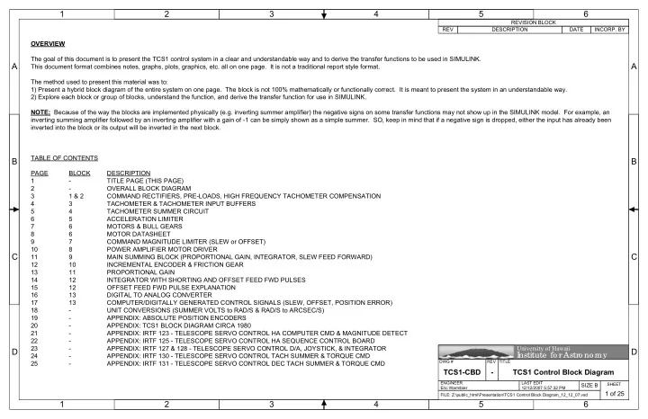
1 2 3 4 5 6 REVISION BLOCK REV DESCRIPTION DATE INCORP. BY OVERVIEW The goal of this document is to present the TCS1 control system in a clear and understandable way and to derive the transfer functions to be used in SIMULINK. A A
1 2 3 4 5 6 REVISION BLOCK REV DESCRIPTION DATE INCORP. BY OVERVIEW The goal of this document is to present the TCS1 control system in a clear and understandable way and to derive the transfer functions to be used in SIMULINK. A A This document format combines notes, graphs, plots, graphics, etc. all on one page. It is not a traditional report style format. The method used to present this material was to: 1) Present a hybrid block diagram of the entire system on one page. The block is not 100% mathematically or functionally correct. It is meant to present the system in an understandable way. 2) Explore each block or group of blocks, understand the function, and derive the transfer function for use in SIMULINK. NOTE: Because of the way the blocks are implemented physically (e.g. inverting summer amplifier) the negative signs on some transfer functions may not show up in the SIMULINK model. For example, an inverting summing amplifier followed by an inverting amplifier with a gain of -1 can be simply shown as a simple summer. SO, keep in mind that if a negative sign is dropped, either the input has already been inverted into the block or its output will be inverted in the next block. TABLE OF CONTENTS B B PAGE BLOCK DESCRIPTION 1 - TITLE PAGE (THIS PAGE) 2 - OVERALL BLOCK DIAGRAM 3 1 & 2 COMMAND RECTIFIERS, PRE-LOADS, HIGH FREQUENCY TACHOMETER COMPENSATION 4 3 TACHOMETER & TACHOMETER INPUT BUFFERS 5 4 TACHOMETER SUMMER CIRCUIT 6 5 ACCELERATION LIMITER 7 6 MOTORS & BULL GEARS 8 6 MOTOR DATASHEET 9 7 COMMAND MAGNITUDE LIMITER (SLEW or OFFSET) 10 8 POWER AMPLIFIER MOTOR DRIVER C C 11 9 MAIN SUMMING BLOCK (PROPORTIONAL GAIN, INTEGRATOR, SLEW FEED FORWARD) 12 10 INCREMENTAL ENCODER & FRICTION GEAR 13 11 PROPORTIONAL GAIN 14 12 INTEGRATOR WITH SHORTING AND OFFSET FEED FWD PULSES 15 12 OFFSET FEED FWD PULSE EXPLANATION 16 13 DIGITAL TO ANALOG CONVERTER 17 13 COMPUTER/DIGITALLY GENERATED CONTROL SIGNALS (SLEW, OFFSET, POSITION ERROR) 18 - UNIT CONVERSIONS (SUMMER VOLTS to RAD/S & RAD/S to ARCSEC/S) 19 - APPENDIX: ABSOLUTE POSITION ENCODERS 20 - APPENDIX: TCS1 BLOCK DIAGRAM CIRCA 1980 21 - APPENDIX: IRTF 123 - TELESCOPE SERVO CONTROL HA COMPUTER CMD & MAGNITUDE DETECT 22 - APPENDIX: IRTF 125 - TELESCOPE SERVO CONTROL HA SEQUENCE CONTROL BOARD 23 - APPENDIX: IRTF 127 & 128 - TELESCOPE SERVO CONTROL D/A, JOYSTICK, & INTEGRATOR University of Hawaii D D I nstitute fo r Astro no my 24 - APPENDIX: IRTF 130 - TELESCOPE SERVO CONTROL TACH SUMMER & TORQUE CMD DWG # REV TITLE 25 - APPENDIX: IRTF 131 - TELESCOPE SERVO CONTROL DEC TACH SUMMER & TORQUE CMD TCS1-CBD - TCS1 Control Block Diagram ENGINEER LAST EDIT SHEET SIZE B Eric Warmbier 12/12/2007 5:57:32 PM 1 of 25 FILE: Z:\public_html\Presentation\TCS1 Control Block Diagram_12_12_07.vsd 1 2 3 4 5 6
1 2 3 4 5 6 7 8 7 (active low) Adj 0 to 8V 7 7 (active low) Adj 0 to 0.5V BUF EAST SLEW DISABLE 0V G=5 SWITCH BUF EAST MOTION DISABLE SWITCH 9 A 13 11 A 14 bit 10 11 1.59 kHz 338 Hz 1.96 .839 PEC B0:B12,B25 (1.33) (1.0) -10 Compensator Digital position DAC Low Pass Low Pass error CMD. 12 12 .002 0 -0.35 V 1 (on output) 12 Adj. pre-load WEST K i = SWITCH RESET ∫ ( ) 2 2 2 Ki v t dt 8 240 Hz 2 2 10 Integrator + + 12 + + G=-2 AMP 0 Half Wave (active low) 12 POSITIVE +8V 12 9 Low Pass Rectifier+ Mag Limit 0 9 9 + LIMIT 338 Hz 9 7 7 5 5 0V 1 0.02 0 5 5 4 + + 11 ADJ 5 11 4.5 468 Hz K i = .839 FD FWD EAST 1 + + 4 SWITCH + - RESET (.513) ∫ + + 1000 1000 + - -1.2 12 ( ) Ki v t dt Low Pass -11 ADJ -11 -4.5 SWITCH + + K i = 680k 330k 1 1 1 Mag Limit Mag Limit Low Pass Mag Limit Mag Limit Integrator 8 + 1 1 10 RESET 240 Hz ∫ ( ) 5 Ki v t dt NEGATIVE 0 + + G=-2 + + AMP Integrator LIMIT 0 Half Wave B 1 B Low Pass Rectifier- Mag Limit 12 SWITCH 12 5 -8V 0 12 EAST 0.35 V 0V 1 0.02 0 (on output) 1 FD FWD WEST SWITCH 5.36 5.36 Adj. pre-load 12 2 1 SWITCH K i = 2 1 RESET ∫ 8.6Hz 240Hz 8.6Hz 240Hz ( ) Ki v t dt Integrator Bandpass Bandpass HA CLEAR INTEGRATOR 9 9 9 2 1 (active low) 338 Hz +8V 6.26 0V (12.1) SLEW EAST/ Low Pass Compensator Compensator SWITCH 3 9 9 723 Hz 9 (active low) 338 Hz -8V 4 6.26 4 0V 3.77 Hz (12.1) 4 Low Pass + SLEW WEST/ SWITCH Low Pass 0.488 3 + 723 Hz Low Pass 9 Joystick (active low) 338 Hz Circuit 4.7 C C 0V (4.7) Low Pass Low Pass SWITCH 9 9 OPPOSING MOTORS - 7 APPLY TORQUE IN .2105 .2105 (active low) 7 3 3 Adj 0 to - 8V ONE DIRECTION ONLY 7 (active low) ~180:1 friction gear ratio Adj 0 to -0.5V 6 (encoder to bull gear) BUF WEST SLEW DISABLE 0V G=5 Tele- SWITCH scope 3 BUF WEST MOTION DISABLE SWITCH Mount EAST MOTOR Tach HA CLEAR INTEGRATOR 144:1 ratio (motor to bull gear) 10 6 Bull gear Incremental Encoder 3 14 WEST MOTOR Tach 3 8 9 1 5 2 D D MECHANICAL Counter + - PEC B0:B12,B25 Active low SLEW signals present when SLEW commanded in a direction. Desired When SLEW is nearly complete and Position SLEW WEST/ deceleration is required, the SLEW signals are removed (high) and the SLEW WEST/ control goes back to standard control. This is based on DIP switch settings HA CLEAR INTEGRATOR representing when to begin SLEW deceleration in number of counts from BUF EAST SLEW DISABLE the end of the SLEW. Integrator is BUF WEST SLEW DISABLE E also shorted during this event. E If an offset is commanded, variable FD FWD EAST amounts of pulses are added to the integrator of opposite polarity to remove charge from the integrator and FD FWD WEST reduce overshoot. F F DWG # REV SIZE SHEET TCS1-CBD - D 2 of 25 1 2 3 4 5 6 7 8
1 2 3 4 5 6 BLOCK GROUP #1 & #2 Inverting Amp with low pass. Half Wave Rectifier Output EAST=negative output (positive for WEST) Gain =-300k/100k =-3 f(-3dB) =1/(2 π RC) Positive Values Only (EAST) =1/(2 π *300k*2200pF) Negative Values Only (WEST) Inverting Amp Gain adjust =240 Hz (Gain = -2) A A Inverting Amp with band pass. Gain =-300k/56k =-5.357 in pass band f(low) =1/(2 π RC) INVERTING =1/(2 π *300k*2200pF) SUMMING =240 Hz ~f(high) =1/(2 π RC) =1/(2 π *56k*0.33uF) =~8.58 Hz Low pass filter Adds a preload to the output f(-3dB) =1/(2 π RC) B B and will be adjusted to add to HOWEVER, the compensation up front =1/(2 π *100*0.1uF) the DAC output about: +0.35V Sets maximum output clamp, will cause lower gain overall and will =16 kHz (East) or -0.35 (West). which must be less than the cause additional lower gain at lower series Zeners, or ~10.7V. frequencies. Also, filter is not a “brick This is really high compared to wall” filter. Pass band will have lower 240 Hz upstream filter. This is gain than calculated as the simulation for high frequency electronic illustrates.. noise induced or picked up. ACTUAL GAIN (input signal is 1V) TRANSFER FUNCTION(S) FOR SIMULINK C C 12 10 Pass band, shorted C8,R33 - - G=-2 + + 0 0 Mag Limit Mag Limit WEST -0.35 Compensated Input Plot from Mathcad Actual circuit 0 0 - - G=-2 + + -12 -10 Mag Limit Mag Limit D D EAST 0.35 DWG # REV SHEET TCS1-CBD - 3 of 25 1 2 3 4 5 6
1 2 3 4 5 6 BLOCK GROUP #3 Identical amplifier input stage for EAST & WEST. TCS Tachometer Voltage vs. Speed Gain= Rf/Rs 10k/47k 2.000 0.213 f(-3dB) =1/(2 π RC) 1.800 y = 0.008845x + 0.005803 =1/(2 π *10k*0.022uF) A A R 2 = 0.999922 =723 Hz 1.600 1.400 y = 0.008764x y = 0.008654x - 0.001271 (Intercept set to Zero) Clamp R 2 = 0.999979 R 2 = 0.999997 East 1.200 West Voltage (V) 1.000 Average Linear (West) 0.800 Linear (East) 0.600 Linear (Average) DIFFERENTIAL AMP w/ filtering 0.400 0.200 B B 0.000 Very high frequency passive filtering 0 50 100 150 200 250 f(-3dB) =1/(2 π RC) -0.200 Where R is the line + source impedance Speed (as/s) which is low. For the tachometer rad/s to volt conversion: NOTE: This conversion is from TELESCOPE sec/ V arc s axis rotational velocity to volts. The = ⋅ Tach sec/ / arc s rad s mechanical model in SIMULINK 0 . 008764 206264.81 sec/ provides axis velocity in rad/s at each V arc s = ⋅ Tach motor geared output (after the 1:144 TRANSFER FUNCTION(S) FOR SIMULINK sec/ / arc s rad s C C ratio). 1807 . 704 V = Tach / rad s Tachometer Velocity (rad) D D DWG # REV SHEET TCS1-CBD - 4 of 25 1 2 3 4 5 6
1 2 3 4 5 6 BLOCK GROUP #4 West Tach IN Gain= -Rf/Rs VEL 4 33.2k/68.1k CMD 4 + - -1.2 -0.4875 f(-3dB) =1/(2 π RC) A A =1/(2 π *33.2k*(1uF+0.27uF) =3.77 Hz West Tach IN 4 4 3.77 Hz + 4 0.488 + Low Pass INVERTING SUMMING East Tach IN w/ filtering Velocity CMD B B INVERTING SUMMING Gain = -120/100 Gain = -1.2 East Tach IN By adding together ~½ of two individual signals, the output is approximately the average. TRANSFER FUNCTION(S) FOR SIMULINK C C NOTE: Be careful with the polarity signs here. The equation will be worked through to demonstrate the polarities. = ⋅ − − VEL 1 . 2 ( _ ) Vout VCMD Vsum amp CMD = ⋅ − − − ⋅ + 1 . 2 ( ( 0 . 4875 ( ))) + - -1.2 Vout VCMD Etach Wtach = ⋅ − + + 1 . 2 ( 0 . 4875 ( )) Vout VCMD Etach Wtach = − − + 1 . 2 ( 0 . 4875 ( )) Vout VCMD Etach Wtach West Tach IN + D D + East Tach IN DWG # REV SHEET TCS1-CBD - 5 of 25 1 2 3 4 5 6
Recommend
More recommend
Explore More Topics
Stay informed with curated content and fresh updates.


