Why Use Scheduling? Sequential accesses to DRAM Memory Access are - PowerPoint PPT Presentation
Why Use Scheduling? Sequential accesses to DRAM Memory Access are wasteful Scheduler Improve latency and bandwidth of memory requests Matthew Cohen, Alvin Lin Order requests to take advantage 6.884 Complex Digital Systems of
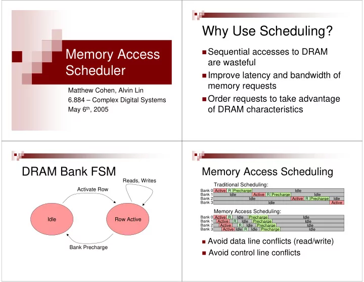
Why Use Scheduling? � Sequential accesses to DRAM Memory Access are wasteful Scheduler � Improve latency and bandwidth of memory requests Matthew Cohen, Alvin Lin � Order requests to take advantage 6.884 – Complex Digital Systems of DRAM characteristics May 6 th , 2005 DRAM Bank FSM Memory Access Scheduling Reads, Writes Traditional Scheduling: Activate Row Bank 0 Active R Precharge Idle Bank 1 Idle Active R Precharge Idle Bank 2 Idle Active R Precharge Idle Bank 3 Idle Active Memory Access Scheduling: Bank 0 Active R Idle Precharge Idle Idle Row Active Bank 1 Active R Idle Precharge Idle Bank 2 Active R Idle Precharge Idle Bank 3 Active Idle R Idle Precharge Idle � Avoid data line conflicts (read/write) Bank Precharge � Avoid control line conflicts
High-Level Architecture Instruction and Data Cache � Separate I- and D-caches Instructions � Fully parameterizable sizes Inst. Cache � Direct mapped caches Controller Memory CPU DRAM � Write-through, no-write-allocate Scheduler Data � Four words per cache line Cache Controller V Tag Word 0 Word 1 Word 2 Word 3 Data V Tag Word 0 Word 1 Word 2 Word 3 V Tag Word 0 Word 1 Word 2 Word 3 Incremental Design Non-Blocking Cache Architecture BUFTAG V0 V1 V2 V3 Tag0Tag1Tag2Tag3 � On cache load miss, � Fully blocking, single word per line BUFTAG V0 V1 V2 V3 Tag0Tag1Tag2Tag3 add request to Pending BUFTAG V0 V1 V2 V3 Tag0Tag1Tag2Tag3 � Fully blocking, four words per line BUFTAG V0 V1 V2 V3 Tag0Tag1Tag2Tag3 Request Buffer (PRB) � Hit under miss � Place µP tag in Tag location, set Valid, issue read � Miss under miss request to scheduler with tag = PRB index � Necessary for full benefits of scheduling � If another read to same line, set tag and valid but no new read request � On return of data, match tag to PRB line, retrieve µ P tag of valid entries, return data to µ P
High-Level Architecture Non-Blocking Cache Architecture Instructions BUFTAG V0 V1 V2 V3 Tag0Tag1Tag2Tag3 � On cache store BUFTAG V0 V1 V2 V3 Tag0Tag1Tag2Tag3 Inst. request, search PRB BUFTAG V0 V1 V2 V3 Tag0Tag1Tag2Tag3 Cache Controller BUFTAG V0 V1 V2 V3 Tag0Tag1Tag2Tag3 � If already issued read Memory CPU DRAM Scheduler to this line, stall Data Cache Controller Data Scheduler Tasks Scheduler Overview � Cache misses are sent to the � Keep waiting buffers of pending memory requests scheduler � Prioritize accesses in waiting buffer � Scheduler is responsible for � Respect timing of the DRAM interfacing with the DRAM � Capture data coming back from DRAM � Requests may be honored out of � Keep the DRAM busy! order
Incremental Design Scheduler RTL Design Waiting Buffer � Blocking In-Order Scheduler Bank 0 Instructions � FIFOs as Waiting Buffers and In- Waiting Buffer Order Scheduling Bank 1 From Cache DRAM Controllers Waiting � Real Waiting Buffers and Data Buffer Bank 2 Interleaved Scheduling Back to Cache Waiting Controllers Buffer Bank 3 Infinite Compile Time Architectural Exploration � Scheduler exploded in complexity � Change cache size to adjust cache miss percentage � Huge amount of combinational logic � Change PRB size to allow for scheduling � Memory access scheduling is a optimization difficult problem � Larger sizes should yield better results but � DRAM is not designed to work easily higher cost with scheduling
Total Time to Make 6000 Random Accesses to 512 Addresses Synthesis Results (Area = 196,117.6 µ m 2 ) 60000 50000 40000 Time (ns) 128 Byte Cache 30000 256 Byte Cache 512 Byte Cache 20000 10000 0 1 10 100 PRB Lines Conclusion Acknowledgements � 6884-bluespec � Memory becoming bottleneck for computer systems � 6884-staff � In-order memory access is simple in logic but wasteful in performance � group1, for teaching us � Memory access scheduling is much more how to use Vector, even if efficient in theory, but complex in you didn’t realize it… implementation
Recommend
More recommend
Explore More Topics
Stay informed with curated content and fresh updates.


![CPU Scheduling Questions Why is scheduling needed? CSCI [4|6] 730 What is](https://c.sambuz.com/961284/cpu-scheduling-questions-s.webp)

