The vertical replacement-gate (VRG) MOSFET J.M. Hergenrother * , - PDF document
Solid-State Electronics 46 (2002) 939950 www.elsevier.com/locate/sse The vertical replacement-gate (VRG) MOSFET J.M. Hergenrother * , Sang-Hyun Oh, T. Nigam, D. Monroe, F.P. Klemens, A. Kornblit Agere Systems, Room 2D-312B, 600 Mountain
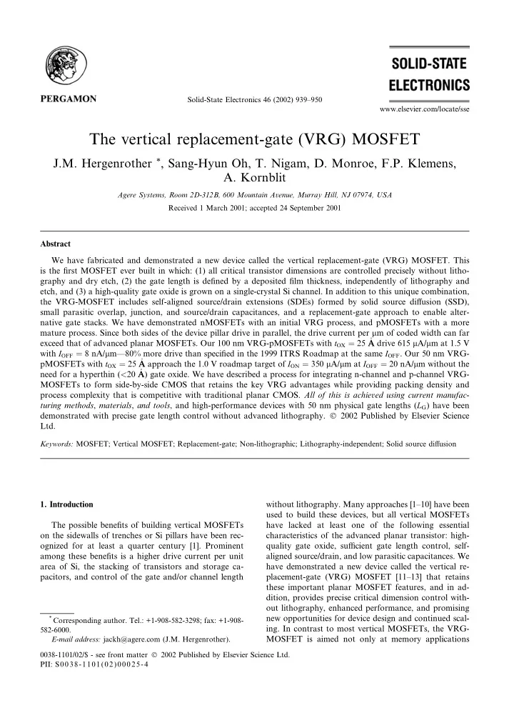
Solid-State Electronics 46 (2002) 939–950 www.elsevier.com/locate/sse The vertical replacement-gate (VRG) MOSFET J.M. Hergenrother * , Sang-Hyun Oh, T. Nigam, D. Monroe, F.P. Klemens, A. Kornblit Agere Systems, Room 2D-312B, 600 Mountain Avenue, Murray Hill, NJ 07974, USA Received 1 March 2001; accepted 24 September 2001 Abstract We have fabricated and demonstrated a new device called the vertical replacement-gate (VRG) MOSFET. This is the first MOSFET ever built in which: (1) all critical transistor dimensions are controlled precisely without litho- graphy and dry etch, (2) the gate length is defined by a deposited film thickness, independently of lithography and etch, and (3) a high-quality gate oxide is grown on a single-crystal Si channel. In addition to this unique combination, the VRG-MOSFET includes self-aligned source/drain extensions (SDEs) formed by solid source diffusion (SSD), small parasitic overlap, junction, and source/drain capacitances, and a replacement-gate approach to enable alter- native gate stacks. We have demonstrated nMOSFETs with an initial VRG process, and pMOSFETs with a more mature process. Since both sides of the device pillar drive in parallel, the drive current per l m of coded width can far exceed that of advanced planar MOSFETs. Our 100 nm VRG-pMOSFETs with t OX ¼ 25 � A drive 615 l A/ l m at 1.5 V with I OFF ¼ 8 nA/ l m — 80% more drive than specified in the 1999 ITRS Roadmap at the same I OFF . Our 50 nm VRG- pMOSFETs with t OX ¼ 25 � A approach the 1.0 V roadmap target of I ON ¼ 350 l A/ l m at I OFF ¼ 20 nA/ l m without the need for a hyperthin ( < 20 � A) gate oxide. We have described a process for integrating n-channel and p-channel VRG- MOSFETs to form side-by-side CMOS that retains the key VRG advantages while providing packing density and process complexity that is competitive with traditional planar CMOS. All of this is achieved using current manufac- turing methods , materials , and tools , and high-performance devices with 50 nm physical gate lengths ( L G ) have been demonstrated with precise gate length control without advanced lithography. � 2002 Published by Elsevier Science Ltd. Keywords: MOSFET; Vertical MOSFET; Replacement-gate; Non-lithographic; Lithography-independent; Solid source diffusion 1. Introduction without lithography. Many approaches [1–10] have been used to build these devices, but all vertical MOSFETs The possible benefits of building vertical MOSFETs have lacked at least one of the following essential on the sidewalls of trenches or Si pillars have been rec- characteristics of the advanced planar transistor: high- ognized for at least a quarter century [1]. Prominent quality gate oxide, sufficient gate length control, self- among these benefits is a higher drive current per unit aligned source/drain, and low parasitic capacitances. We area of Si, the stacking of transistors and storage ca- have demonstrated a new device called the vertical re- pacitors, and control of the gate and/or channel length placement-gate (VRG) MOSFET [11–13] that retains these important planar MOSFET features, and in ad- dition, provides precise critical dimension control with- out lithography, enhanced performance, and promising * Corresponding author. Tel.: +1-908-582-3298; fax: +1-908- new opportunities for device design and continued scal- ing. In contrast to most vertical MOSFETs, the VRG- 582-6000. E-mail address: jackh@agere.com (J.M. Hergenrother). MOSFET is aimed not only at memory applications 0038-1101/02/$ - see front matter � 2002 Published by Elsevier Science Ltd. PII: S0038-1101(02)00025-4
940 J.M. Hergenrother et al. / Solid-State Electronics 46 (2002) 939–950 Fig. 1. Outline of the VRG process. but also at high-performance random logic and high- 3. Solid source diffusion speed applications. Since the vertical VRG geometry precludes the use of ion implantation in the formation of self-aligned SDEs, SSD is another key enabling element of the VRG pro- 2. Basic VRG process cess. SSD allows us to form self-aligned SDEs in this novel geometry, and it therefore transforms the precise The basic ideas of the VRG process are illustrated in gate length control afforded by the VRG process into Fig. 1. A multilayer stack that contains a sacrificial gate precise, lithography-independent channel length control. layer and two dopant source layers is deposited. A In the SSD technique, dopants from highly doped trench is etched through this stack and it is filled with phosphosilicate glass (PSG) or borosilicate glass (BSG) single-crystal Si to form the device channel. Shallow, diffuse into adjacent silicon to form self-aligned, shallow self-aligned source-drain extensions (SDEs) are formed SDEs. Several groups have demonstrated competitive by solid source diffusion (SSD) from the dopant sources. planar MOSFETs with ultrashallow junctions formed The sacrificial gate layer is subsequently removed, a gate by SSD [14–17]. The dopant concentration in the silicon oxide is grown on the exposed portion of the channel, is determined by its concentration in the oxide, the do- and the gate is deposited in place of the sacrificial layer. pant diffusivity in the oxide as well as in the silicon, The key enabling element of the VRG process is its re- the segregation at the interface, and the character of placement-gate approach — this allows for the fabrica- the interface. We can obtain shallow junctions with tion of high-quality gate oxides on a vertical {1 0 0} Si low sheet resistances using SSD without having to con- surface whose length is defined by a film thickness. This cern ourselves with channeling effects and TED associ- flow should be mechanically scalable to sub-30 nm gate ated with implant damage. lengths with excellent (3 r < 3%) control. Table 1 sum- Fig. 2 shows 1-dimensional SIMS profiles of phos- marizes the important features of the VRG process phorus SSD driven by rapid thermal anneal (RTA). along with some of the promising device design oppor- Blanket PSG films with 4 wt.% phosphorus (1 : 8 � 10 21 P tunities that it creates. atoms/cm 3 ) were deposited by PECVD at 400 � C using TEOS, O 2 , and trimethyl phosphine on an initially hy- Table 1 drogen terminated {1 0 0} silicon surface. The wafers Summary of important VRG process and device features were subsequently annealed at either 1000 or 1050 � C to � All critical dimensions controlled precisely without form shallow n+ junctions. Although these profiles lithography and dry etch represent respectable n+ junctions, the surface concen- � Gate length controlled by film thickness trations do not show a solubility-limited value. This may � High-quality gate oxide grown on epi Si channel be due to: (1) interface effects that could be specific to � Self-aligned SDEs formed by SSD these 1-dimensional, blanket-wafer SSD experiments, or � SOI-like parasitic capacitances (2) the depletion of phosphorus in the doped oxide near � Replacement-gate enables alternative gate stacks the interface due to the relatively slow diffusion of � Device free from substrate — increases design flexibility phosphorus in the oxide. More experiments and mod- � Epi channel plus CMP opens door to 3D integration eling work are under way to improve the surface con- � Vertical design enables graded channel doping � Offset spacers controlled by film thicknesses centration and junction profiles for these n+ junctions. � Short-channel performance independent of deep source/ Fig. 3 shows SIMS profiles of boron SSD from highly drain depths doped (5 wt.% boron), blanket BSG dopant sources � Made with production tools, methods, materials for different RTA conditions. In contrast to the n+
J.M. Hergenrother et al. / Solid-State Electronics 46 (2002) 939–950 941 Fig. 2. SIMS profiles of phosphorus SSD driven by RTA. Fig. 3. SIMS profiles of boron SSD driven by RTA. Compet- itive, solubility-limited profiles with steep gradients were ob- junctions of Fig. 2, these profiles represent competitive, tained. shallow p+ junctions. For boron SSD, we have obtained solid-solubility limited, steep (9 nm/dec), box-like junc- boron-doped epitaxial Si device channel was grown se- tions with low sheet resistances. lectively in this trench (Figs. 6 and 7) by RTCVD at 850 � C using dichlorosilane and HCl. The growth time was chosen so that the trenches were completely filled (i.e. 4. Device fabrication of initial VRG-nMOS there was epitaxial lateral overgrowth around the entire perimeter of the trench). The channel was then plana- The VRG process was first demonstrated with n- rized to the top nitride layer by CMP (Fig. 8). The channel devices [11]. The process used to fabricate these undoped oxide film in the stack was a sacrificial layer nMOSFETS is shown in Fig. 4. Arsenic was implanted whose thickness defined the gate length L G , the two into an epi Si wafer to form the device drain and a thin PSG layers were dopant sources used to form low-re- oxide diffusion barrier was deposited. A PSG/nitride/ sistance, shallow, self-aligned SDEs by SSD of phos- undoped oxide/nitride/PSG/nitride stack was deposited phorus. The phosphorus concentration in these PSG and a trench (or window) with nearly vertical sidewalls layers was 4 wt.%. The thin nitride layers between the was etched through the entire stack (Fig. 5). The in-situ undoped oxide and the dopant sources functioned as Fig. 4. Process flow used to fabricate the initial VRG-nMOSFETs.
Recommend
More recommend
Explore More Topics
Stay informed with curated content and fresh updates.


