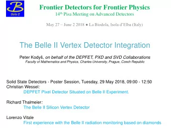
The DEPFET pixel detector for BELLE II 8 th International Hiroshima - PowerPoint PPT Presentation
LMU Mnchen - Excellence Cluster Universe The DEPFET pixel detector for BELLE II 8 th International Hiroshima Symposium on Development and Application of Semiconductor Tracking Detectors Stefan Rummel on behalf of the DEPFET Collaboration
LMU München - Excellence Cluster Universe The DEPFET pixel detector for BELLE II 8 th International “Hiroshima” Symposium on Development and Application of Semiconductor Tracking Detectors Stefan Rummel on behalf of the DEPFET Collaboration Stefan.Rummel@lmu.de
DEPFET collaboration • Charles University, Prague DEPFET collaboration was • DESY Hamburg established for ILC-Vertexing, in 2009 moved towards BELLE II • IFIC Valencia • IFJ PAN, Krakow DEPFET community still grows! • IHEP, Bejing • LMU Munich • TU Munich • MPI Munich / HLL • University of Bonn • University of Heidelberg • University of Giessen • University of Göttingen • University of Karlsruhe Stefan Rummel 2
BELLE II / SuperKEKB – Latest news On 18.11.11: • SuperKEKB ground breaking ceremony • MoU between KEK and German funding agencies signed Stefan Rummel 3
Overview • Introduction • SuperKEKB and BELLE II • DEPFET concept • Working principle • The DEPFET-PXD system • R&D • Mechanics and services • System and DAQ • Readout chips • Test Beams • Power distribution system • Requirements • System Layout • Performance • Outlook Stefan Rummel 4
SuperKEKB upgrade • Luminosity / precision frontier Looking for new physics in the loops • 10.4GeV @ Y(4S) resonance • SuperKEKB asymmetric e+/e- collider B-Mesons with boost in lab frame • Nano beam option + increased current Accelerator upgrade to 8x10 35 1/cm 2 /s Stefan Rummel 5
BELLE II upgrade • High luminosity poses challenges for all sub detectors • Upgrade of data acquisition • Performance improvements in sub detectors • Inner detector: • Silicon strip detector suffers under high occupancy • Two layers of pixel detector (PXD) • In total 6 Silicon layers Challenges to the PXD: • High interaction rate • Radiation hardness of ~1 MRad/y • High precision High readout speed Low mass, high resolution Stefan Rummel 6
The DEPFET - Active Pixel Detector Dep leted F ield E ffect T ransistor • In pixel amplification of charge • Potential minimum under gate • Electrons modulate current in FET • Charge is removed via clear Low input capacity Fully depleted operation - high sensitive volume Charge collection always active DEPFET allows to build low mass, high S/N detector! Stefan Rummel 7
The DEPFET - Technology DEPFET is developed and produced at MPI - Semiconductor lab (HLL) in Munich: • Double sided process on high resistivity silicon • Detectors on wafer scale • Thinning technology available Low leakage current 450 m m Flexible size 50 m m Low multiple scattering Stefan Rummel 8
The DEPFET – Matrix operation DEPFET pixel cell arranged on grid • • Readout • Rolling shutter mode • Correlated Double Sampling / Single Sampling Frame time 20µs – 92ns row processing time • Column parallel readout – fast readout Low power dissipation in active area Stefan Rummel 9
BELLE II DEPFET-PXD • PXD in a nutshell: • Radius: 14,22mm • Pixel size 50x50µm², 50x75µm² • Pixel: 8M • Thickness: 75µm • Radiation hardness: 10MRad • Frame time: 20µs • Material budget: 0.2% X 0 DEPFET PXD will significantly improve z- vertex resolution of the inner detector Stefan Rummel 10
Mechanical Engineering • Engineering challenges: • Stable mounting - vibration • Cooling • Services in/out • Tight mechanical constraints: • Beampipe @ 12mm radius • SVD @ 38mm radius • Active area cooled by cold air Data and heat is generated at the end of module – outside the acceptance! Stefan Rummel 11
Mechanical Engineering Stefan Rummel 12
System layout • Zero suppression on module level • Online pattern recognition to reject background • Online silicon only tracking ~80Gbit/s 0 ~15m ~4Gbit/s ~40cm 4 links @ 1.25Gbit/s Stefan Rummel 13
System layout – Readout and steering chips DCDB DHP Switcher Amplification and digitization of Signal processor Control of gate and clear DEPFET signals Common mode correction 32 x 2 channels 256 input channels Pedestal subtraction Switches up to 30V 8-bit ADC per channel 0-supression 0.35 µm HV technology 92 ns sampling time Timing and trigger control 180 nm technology 90nm technology Stefan Rummel 14
DEPFET test beam • Testbeam CERN 10/2011: • 50µm thin DEPFETS • 92ns row processing time • DUTs: • L=4 µm , standard oxide: SNR ~40 • L=6 µm , thin oxide: SNR ~ 20 • Resolution: 12.4µm Full readout speed and first thin DEPFET in TB Stefan Rummel 15
Power distribution requirements Steering voltages : • Around 20 voltages are needed • Steering/Biasing voltages for the DEPFET • Fine tuning for optimization • Parameter changes due to irradiation • Precise hardware current limit • Bipolar and sink/source output needed • Low noise essential for SNR • Supply voltages for the ASICs • Sub-micron chips sensitive to over voltage • Sink/source output needed Frontend voltages : • Need control on transient behavior of PS-system • Several dependencies between voltages • Dedicated power up and down sequences Development of a dedicated low noise power supply system Stefan Rummel 16
PS System – Architecture Stefan Rummel 17
PS System – Low noise operation • Low noise essential for successful operation • Efficiency / spatial resolution • dE/dx resolution • E.g. Gate_ON voltage: g m ~20-40µS 1mV rms 20-40nA rms ≈ Frontend noise! Low PS noise crucial for PXD operation How to get low noise at module level? 1. Control emission of PS 2. Shield the system from interference 3. Close current loops locally Stefan Rummel 18
PS System – Low noise operation • PS level • Remote sensing with long lines Can’t count on PSRR • DC/DC converter with broadband filtering • Physically separate converter from regulators • Additional output filtering • Power distribution: • Cabling with combined braid/foil shield • Common mode and differential mode close to detector • Lines sharing a common impedance lead to intrinsic noise due to varying load current • Close current loops locally • Assure low output impedance at load for all frequencies Project to investigate EMC compatibility on PXD level has been started Stefan Rummel 19
PS System – Output impedance Hierarchical approach – based on available space: • Low frequencies ( dc ~ 20kHz): Regulator is active • Mid frequencies (20kHz-~MHz): Decoupling on PP level • High frequencies (>~MHz): Decoupling on module level ~5uH ~20nH Stefan Rummel 20
PS System – Output impedance ESL, L(PCB) dominates • Spice simulation of regulator and cables • Measurement with regulator Dip: ESR of C and PCB PP Decoupling Module level Amplifier Output impedance is kept low takes effect Takes effect roll off over a wide frequency range Careful layout necessary to control resonances Stefan Rummel 21
Summary • The KEKB accelerator is upgraded towards 8x10 35 /cm²/s • A 2 layer pixel detector based on DEPFET will be installed • Design of PXD is well advanced • DEPFET pixel cell, radiation hardness • Mechanical design and cooling • Readout electronics and data acquisition • TB program ongoing • Readout speed and thin DEPFET sensors demonstrated in test beam Design of a dedicated PS system for the DEPFET PXD is ongoing, first • prototype has been tested • PXD ready by mid 2015 Stefan Rummel 22
Backup Stefan Rummel 23
Schedule Stefan Rummel 24
CP – Violation What do we measure? Precise Vertex detectors essential to measure CP violation! 25 Stefan Rummel
Physics motivation • NP can visible via loop corrections • Suppressed decay of K 0 lead to forecast of Charm • Top mass was known before discovery • Example: Models with charged Higgs doublet (2HDM-II): B + → τ + ν Γ (B + → τ + ν ) = Γ SM (B + → τ + ν ) [1-(m b /m H )²tan² ϐ ]² • Energy reach far beyond E cms red: 5 σ discovery region @5ab -1 26 Stefan Rummel
Power supply transient response • Load transients of readout chips lead to dangerous overvoltage spikes • Limits of overvoltage have been derived for 180nm/90nm technology Overvoltage can be controlled by capacitors close to the load 15m, 2.5A,100nF 15m, 2. 15m, 2.5A,10µF Stefan Rummel 27
Thinning Technology sensor wafer sensor wafer handle wafer handle wafer etching of handle Wafer bonding Thinning of top Processing wafer (structured) wafer (CMP) SOI process Stefan Rummel 28
Recommend
More recommend
Explore More Topics
Stay informed with curated content and fresh updates.
