Sub-Micron Lithography with the Sub-Micron Lithography with the - PowerPoint PPT Presentation
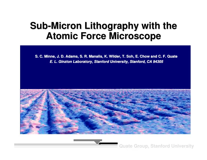
Sub-Micron Lithography with the Sub-Micron Lithography with the Atomic Force Microscope Atomic Force Microscope S. C. Minne, J. D. Adams, S. R. S. C. Minne, J. D. Adams, S. R. Manalis Manalis, K. Wilder, T. , K. Wilder, T. Soh Soh, E. Chow
Sub-Micron Lithography with the Sub-Micron Lithography with the Atomic Force Microscope Atomic Force Microscope S. C. Minne, J. D. Adams, S. R. S. C. Minne, J. D. Adams, S. R. Manalis Manalis, K. Wilder, T. , K. Wilder, T. Soh Soh, E. Chow and C. F. , E. Chow and C. F. Quate Quate E. L. E. L. Ginzton Ginzton Laboratory, Stanford University, Stanford, CA 94305 Laboratory, Stanford University, Stanford, CA 94305 Quate Group, Stanford University
CD Control Requirements CD Control Requirements I The 1997 SIA Roadmap for Semiconductors predicts strict CD The 1997 SIA Roadmap for Semiconductors predicts strict CD I tolerances as linewidths linewidths shrink: shrink: tolerances as 3 σ CD Tolerance Year Feature Size 2001 150 nm ± 12 nm 2003 130 nm ± 10 nm 2006 100 nm ± 7 nm 2009 70 nm ± 5 nm 2012 50 nm ± 4 nm I This trend presents a variety of challenges: • resolution • pattern transfer capabilities (selective, anisotropic etches) • uniformity (along features and • pattern placement (overlay across fields & wafers) registration) • repeatability (process latitude) • throughput Quate Group, Stanford University
Atomic Force Microscope Atomic Force Microscope Optical Lever (A - B) Laser Detection A B Feedback Control Sample Display Actuator Driver X Y Z Actuator Quate Group, Stanford University
Throughput Requirements Throughput Requirements for Sub-Micron Lithography with the Atomic Force Microscope I Goals Goals I – – 200 mm wafer 200 mm wafer 13 50nm pixels per wafer – – 10 10 13 50nm pixels per wafer – 10 wafers per hour 10 wafers per hour – I Required Capabilities Required Capabilities I – 10 mm/s scan speed 10 mm/s scan speed – – 5 probes per mm 5 probes per mm 2 2 – I Achievements Achievements I – 10 mm/s scan speed (optical lever) – 10 mm/s scan speed (optical lever) – – 32 tips in parallel ( 32 tips in parallel (piezoresistor piezoresistor) ) – 5 probes per linear mm (PR + 5 probes per linear mm (PR + ZnO ZnO) ) – 2 image ( – – 4 mm 4 mm 2 image (piezoresistor piezoresistor) ) – – Arbitrary pixels up to 100 Arbitrary pixels up to 100 MBytes MBytes Quate Group, Stanford University
Array of 50 Cantilevers with Array of 50 Cantilevers with Integrated Sensors & Actuators Integrated Sensors & Actuators Piezoresistor ZnO Actuator ZnO Ground Bus Piezoresistor Ground Bus Individual Cantilever’s. . . Piezoresistive Sensor Output ZnO Actuator Input Lithography Write Input Quate Group, Stanford University
High Speed Atomic Force Microscopy High Speed Atomic Force Microscopy 10 piezo tube Amplitude (arb) 1 ZnO 0.1 0.1 1 10 100 Drive Frequency (kHz) Quate Group, Stanford University
2 mm x 2mm Parallel AFM Image 2 mm x 2mm Parallel AFM Image 200 um 2 mm 10 tips in parallel at 1mm/s. No feedback. Quate Group, Stanford University
32 Images over 6.4 mm 32 Images over 6.4 mm Automated Data Acquisition, Constant Height 200 um 1 8 16 9 17 24 25 32 Quate Group, Stanford University
Throughput Requirements Throughput Requirements for Sub-Micron Lithography with the Atomic Force Microscope I Goals Goals I – – 200 mm wafer 200 mm wafer 13 50nm pixels per wafer – – 10 10 13 50nm pixels per wafer – 10 wafers per hour 10 wafers per hour – I Required Capabilities Required Capabilities I – 10 mm/s scan speed 10 mm/s scan speed – – 5 probes per mm 5 probes per mm 2 2 – I Achievements Achievements I – 10 mm/s scan speed (optical lever) – 10 mm/s scan speed (optical lever) – – 32 tips in parallel ( 32 tips in parallel (piezoresistor piezoresistor) ) – 5 probes per linear mm (PR + 5 probes per linear mm (PR + ZnO ZnO) ) – 2 image ( – – 4 mm 4 mm 2 image (piezoresistor piezoresistor) ) – – Arbitrary pixels up to 100 Arbitrary pixels up to 100 MBytes MBytes Quate Group, Stanford University
Uniform High Aspect Ratio Tall Tips for Uniform High Aspect Ratio Tall Tips for Large Arrays Large Arrays I Uniform tips allow for Uniform tips allow for I larger arrays larger arrays I Tall tips facilitate 2-D Tall tips facilitate 2-D I imaging imaging I High aspect ratio tips for High aspect ratio tips for I demanding applications demanding applications Quate Group, Stanford University
Through-Wafer Metal Through-Wafer Metal Interconnection Interconnection L Goal Goal L Through-wafer Electrical Through-wafer Electrical Interconnection for 2 Dimensional Interconnection for 2 Dimensional Array Addressing. Array Addressing. L Processing Techniques Processing Techniques L Through-wafer anisotropic RIE etching Through-wafer anisotropic RIE etching G G of 30um vias vias. (AR > 18:1) . (AR > 18:1) of 30um Oxide Insulation. Oxide Insulation. G G CVD Metalization Metalization. . CVD G G Metal Patterning using Metal Patterning using electro electro- - G G deposited Photoresist deposited Photoresist. . Quate Group, Stanford University
Isolation and Metallization Metallization of Deep Trenches of Deep Trenches Isolation and Cross Sectional SEM Micrograph Top Side Middle of Wafer Quate Group, Stanford University
SAL601 Exposure and Etch SAL601 Exposure and Etch Expose with EBL or SPL: e- 65 nm SAL601 silicon SAL601 430 nm Resist Develop in MF-322: Etch in high density plasma (HBr + O 2 ) : 600 nm Etched Silicon Quate Group, Stanford University
Scanning Probe Lithography (SPL) Scanning Probe Lithography (SPL) FORCE FEEDBACK CURRENT F FEEDBACK deflection sensor current z piezo tube amplifier signal [v] laser detector xyz scanner cantilever tip resist I sample bias stage Quate Group, Stanford University
EBL Proximity Effects EBL Proximity Effects I Patterns printed with EBL in Patterns printed with EBL in I Pixel SAL601 with a 40 nm SAL601 with a 40 nm pixel spacing pixel spacing and etched into Si Si Width: 1 2 3 4 and etched into – – Isolated single pass line is 120 nm Isolated single pass line is 120 nm wide wide – – 4-pixel-wide feature has width greater 4-pixel-wide feature has width greater than four times the width of the single than four times the width of the single pass line pass line – – Lines on 500 nm Lines on 500 nm pitch are resolved but pitch are resolved but are wider than isolated lines are wider than isolated lines – – No lines on 200 nm No lines on 200 nm pitch are resolved pitch are resolved 500 nm pitch 200 nm pitch 7.5 µm Quate Group, Stanford University
SPL Linearity SPL Linearity 37 nm 239 nm Pixels: 1 2 3 4 5 6 300 nm 40 nm Exposure Dose=20 nC/cm Quate Group, Stanford University
SPL Linewidth Linewidth Control Control SPL 600 nm 430 nm 150 nm 1 µm 1 µm 1 µm Linewidth=65 nm Quate Group, Stanford University
SPL Resolution & Transfer SPL Resolution & Transfer 6:1 Aspect Ratio 10:1 Aspect Ratio 6:1 Aspect Ratio 10:1 Aspect Ratio Linewidth=26 =26 nm nm Linewidth=50 =50 nm nm Linewidth Linewidth SAL601 Exposure PMMA Exposure, SAL601 Exposure PMMA Exposure, & Etch Lift-Off, & Etch Lift-Off, & Etch & Etch 120 nm 200 nm Quate Group, Stanford University
Non-Contact AFM Lithography Non-Contact AFM Lithography setpoint error current signal ADC differential DSP amplifier piezo tube trans-impedance actuator amplifier cantilever measured tip current resist bias silicon stage Quate Group, Stanford University
Developed Resist Features Developed Resist Features AFM image of SAL601 AFM image of SAL601 I I resist patterns exposed resist patterns exposed in the non-contact AFM in the non-contact AFM mode mode Image taken in the Image taken in the I I tapping AFM mode with tapping AFM mode with the same cantilever the same cantilever used for patterning used for patterning Resist features are 65 Resist features are 65 I I nm nm tall and about 30 tall and about 30 nm nm wide wide Quate Group, Stanford University
Etched Lines Patterned by Etched Lines Patterned by Non-Contact AFM Lithography Non-Contact AFM Lithography Features are 28 nm nm wide near the center of the lines and 32 wide near the center of the lines and 32 nm nm Features are 28 I I wide near the ends wide near the ends Lines were etched 320 nm Lines were etched 320 nm deep into the silicon, giving an deep into the silicon, giving an I I aspect ratio of about 10:1 aspect ratio of about 10:1 Quate Group, Stanford University
Recommend
More recommend
Explore More Topics
Stay informed with curated content and fresh updates.
