STT read-out Detectors requirements and layout Read-out concept - PowerPoint PPT Presentation
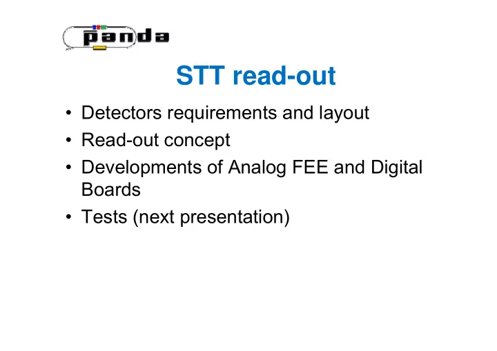
STT read-out Detectors requirements and layout Read-out concept R d t t Developments of Analog FEE and Digital p g g Boards Tests (next presentation) Tests (next presentation) PANDA STT Central tracker : 4636
STT read-out • Detectors requirements and layout • Read-out concept R d t t • Developments of Analog FEE and Digital p g g Boards • Tests (next presentation) • Tests (next presentation)
PANDA STT • Central tracker : 4636 straws • Forward tracker : ~13500 straws F d t k 13500 t • Drift time ~ 200 ns • Time measurement : req. electronic resolution < 1 ns • sensitivity (threshold) ~ 2 fC sensitivity (threshold) 2 fC • dE/dx, Q for PID : MIP: 5*10 6 e - , signal charge 10 6- 10 8 e - PID (Central tracker): 10% resolution in 24 layers PID (Central tracker): 10% resolution in 24 layers • detector capacitance: ~ 10-15 pF (9 pF/m) • Hit rates up to 800 kHz/channel
Expected rates p beam = 15 GeV/c, N Int =2x10 7 s -1 . Hit rate/cm/event in Central STS Forward STS 10 -3 M Max rate: ~400 kHz for STS3 t 400 kH f STS3 Max rate: ~ 5kHz/cm -> ~800 kHz for 150cm long tube
Central Tracker
5-8 m
PANDA DAQ PANDA DAQ epoques (i.e 500 μ s) μ ) p q (
Read-out concepts Read-out concepts • Complete read-out on detector Co p e e ead ou o de ec o • avaliable space Δ L <15 cm A<4000 cm 2 • rad. hardness (FPGA’s in digital part ?!) d h d (FPGA’ i di it l t ?!) • cooling system needed • Compact analog part on detector (ASIC) (available space ~40 cm 2 for 16 channels) • digital part (TDC/ADC) 5-8 m away outside detector • nGbit/s links to Panda network
Straw tubes read-out chain FE cards : Preamp+ Shaper+ BLR + Discriminator • Dynamic Range ~ 5fC - 1pC, noise <1 fC FE • Peaking time ~10-15 ns, Peaking time 10 15 ns • Signal duration < 100 ns (pile-up < 10% @ 800 kHz) • Gain 10-15 mV/fC DB Digital Boards Common Clock Common Clock • Multihit TDC : Time measurement + TimeOverThreshold (TOT) M ltihit TDC Ti t + Ti O Th h ld (TOT) Distribution for charge measurement OR/AND signal after shaper as input to (i.e SODA) FADC • binning 0.5-0.8 ns Panda DAQ - network • Zero suppression & Hit detection.. Slow /Run/Data flow control Data Concentration : • gathering and sorting of hits marked by time stamps in epoques (i.e 500 μ s bunch) epoques (i.e 500 μ s bunch) • nGbit/s Optical serial link
Developments p • Concept based on TDC +(ADC?)-Kraków (AGH, JU/GSI) JU/GSI) • New dedicated analog ASIC (preamp+shaper+discriminator) Dominik Przyborowski/Marek Idzik (AGH) P b ki/M k Id ik (AGH) • TRBv2: TDC : HPTDC (CERN) TRBv2 – existing: can be used for detector tests with trigger rates up to 50 kHz • TRBv3: TDC in in FPGA (new)- TRB v3 – designed to fit also Panda spec. ( ) g (M.Traxler/J.Michel/M.Pa ł ka/M.Kajetanowicz/G. Korcyl) • • TOT: amplitude measurement via width of signal above threshold (TDC) TOT: amplitude measurement via width of signal above threshold (TDC) or • ADC ADC: charge measurement in FADC (~100 MHz) – h t i FADC ( 100 MH ) as Addon card on Add d TRBv3 –discussion is on-going
New ASIC for Panda STS Prototype I (july 2011) : in tests Evaluation board
TDC operation mode & data volume measurement range measurement range clock (1MHz) clock (1MHz) T time ti • 1 MHz trigger clock (derived from SODA) •: TDC with 0.5 ns binning: time 1 μ s range: 11 bits TOT 200 ns : 8 bits channel number(1-32): 5bits time stamp (i.e 1-500); 8 bits TDC id, +trailer/header ~ 5 bytes/hit • Data volume: 32 channels TDC @ max 800 kHz hit rate/channel -> ~128 MB/s • Data buffer : 32 channels TDC (i.e for 500 μ s epoque): 64-80 kB
step I (done): Trigger and Read-out Board • TRBv2 board developed by HADES DAQ group • many boards TRB v2 installed and used in the HADES DAQ � 128 TDC h � 128 TDC channels (HPTDC) l (HPTDC) � 130 MB/s data throughput achieved via optical links with TRBnet (8/10B i (8/10B in 2 Gbit/s) 2 Gbit/ ) � TRBnet protocol (FPGA): 3 logical channels; data transport, slow control run control control, run control
TRBv2 • 128 TDC channels 128 TDC channels (100ps, 192ps, 780 ps) TDC 2, 3 TDC 2, 3 • 2.5 Gb/s serial 8/10b Optical link Optical link SDRAM SDRAM link TDC TDC 0, 1 0, 1 , FPGA: TDC control + FPGA FPGA TrbNet Virtex4 Virtex4 DSP DSP •Data flow control • Slow control • Run control ETRAX SDRAM ETRAX ETRAX ETRAX DC/DC DC/DC DC/DC DC/DC SDRAM Ethernet Ethernet Ethernet Ethernet Marek Palka, GSI 13
more powerfull: TRBv3 p • 4 TDC in FPGA ( Lattice ECP3M) up to 256 TDC channels channels 4Mbit memory (enough to store one 0.5 ms bunch ) • 1 FPGA for control (Run, Data, Slow-control) • up to 8 x 3.2Gbit/s (8/10b) serial links for data transmission (enough to send data from 256 channels with 0.8 MHz hit rate) • interface for Add-on connectors : i.e ADC t i ADC • ~ 20 W power
Status TRB v3 Status TRB v3 • • Board produced and has Board produced and has all basic functionality (FPGA programming etc ) etc.) • GbEth alreay implemented and connection to Compute Node established (G.Korcyl) ( y ) • TDC firmware is ongoing (GSI/M.Pa ł ka (UJ)) • TRB TRBnet in progress t i (J.Michel/U.Frankfurt)
back up slides back-up slides
TOT– energy loss : HADES MDC measured: (J. Markert/ A.Schmah –U. Frankfurt) • dE/dx vs impact angle • dE/dx vs impact angle 24 * ~7 mm gaps He:Iso (2:1) FEE based on ASD8 chip
Recommend
More recommend
Explore More Topics
Stay informed with curated content and fresh updates.
