Stress-strain curves derived from continuous nano-indentation of - PDF document
18 TH INTERNATIONAL CONFERENCE ONCOMPOSITEMATERIALS Stress-strain curves derived from continuous nano-indentation of W-C-N films Soo In Kim 1 , Kyu Young Lee 1 , Joo Young Kim 1 , Hwan Won Oh 1 , Hyun Woo Kim 2 , and Chang Woo Lee 1 * 1 Nano &
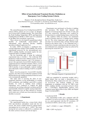
18 TH INTERNATIONAL CONFERENCE ONCOMPOSITEMATERIALS Stress-strain curves derived from continuous nano-indentation of W-C-N films Soo In Kim 1 , Kyu Young Lee 1 , Joo Young Kim 1 , Hwan Won Oh 1 , Hyun Woo Kim 2 , and Chang Woo Lee 1 * 1 Nano & Electronic Physics, Kookmin University, Seoul 136-702, Korea 2 Korea Advanced Institute of Science and Technology, Dajeon, 305-701, Korea * Corresponding author: cwlee@kookmin.ac.kr Keywords : W-C-N diffusion barrier, indentation, stress-strain curve, stress – depth curve In semiconductor metallization processes, diffusion barrier is essential for preventing diffusion between metal (Cu: copper) and Si (silicon). However, the Cu has some problems such as easy reaction, poor adhesion, and diffusion into Si. In this study, we suggest tungsten -carbon -nitride (W-C-N) thin films for diffusion barrier that were made by rf magnetron sputtering. Subsequently, heat treatments execute as high temperature up to 800 ℃ .The films were analyzed continuous stress – strain test according to depth (from surface to Si substrate) by in-situ nano-indenter. The elastic modulus (Er) and hardness (H) of W-C and W-C-N thin films are changed from 152.08 to 168.31 GPa and from 12.05 to 13.2 GPa, respectively. After annealing at 800 ℃ , the Er and H values are decreased compared with as-deposited state of W-C and W-C-N films from 105.1 to 131.31 GPa and 2.25 to 11.9 GPa, respectively. From the stress – depth graph, the W-C-N thin film was more stable than that of W-C film after annealing up to 800 ℃ . From these results, the W- C-N thin film is more effective to prevent interdiffusion between Cu and Si. state annealing for various annealing temperature 1. Introduction (up to 800 ℃ ). Also, the Nano-indentation system Through the rapid development of electronic was used for analyzing the deformational industry, the machines and electronic appliances characteristics of W-C-N thin film such as yield need nano-size line width device. The Al (aluminum) points, hardness, and surface stability. interconnects have been primarily used for circuit lines but the specific resistance of Al has a higher value than that of Cu (copper). Therefore, copper 2. Experimental has been used to construct circuit lines for devices There is a way to understand the features of the with narrower line width. However, the Cu has some surface called uniaxial compressing test. In this test, problems such as reaction with Si easily, poor the stress only occurs in one direction; compressive adhesion, and diffusion into the substrate of Si or tensile. During the indentation test, the stress (silicon). So we suggest tungsten related diffusion occurs in every direction. However, there is a barrier added impurities to insert between Cu and Si similarity between compressive or tensile tests [1-3]. The barrier has low sheet resistance and not to when analyzing the results, compressive or tensile react with Si and Cu for high temperature annealing methods also need to transform the load - depth process. graphs to stress - h C graphs (where h C is content In this paper, the W-C-N diffusion barrier was depth). In the stress - h C curves, the stress means the deposited by rf magnetron sputtering method and it pressure of the indenter and the h C means the contact needs to be characterized. Recently, we have been depth of indenter [4]. measured through spectroscopy equipments such as XRD (X-Ray Diffraction), XPS (X-ray F ���� Indentation Stress � σ � � � � (1) Photoelectron Spectroscopy) and so on. These measurement methods are average value of sample From the load - depth graph, we can get the value of spot about over than micro meter’s area in macro F Load . The evaluation of the stress requires scale. knowledge of both the applied force F Load and the Thus, we study the nano-surface properties of W- projected contact area A C . During the indentation, C-N diffusion barrier according to the concentration A C is computed from the contact depth (h C ). The of nitrogen impurities of as-deposited and annealed
contact depth h C is earned through the equation (2) sample. Indentation was executed 16 times per each [3-6]. sample and thus, totally 64 indentations were performed. � ���� � � � � � � (2) � 3. Result and Discussion ( � : geometrical constant of the tip, S : stiffness) Figure 1 shows the load force - depth graphs that the indentation datas are almost the same in sample Because we used the Berkovich tip, the value of � is 1, 3 (W-C and W-C-N thin films for as-deposited about 0.75. Stiffness is defined as the initial slope of state), and 4 (W-C-N thin film for annealed state). the unloading curves like (3) [5-6]. On the other hand, the result of sample 2 (W-C thin film after annealed) is move back and it means that � ���� Stiffness �S� � �� (3) the hardness value of sample 2 is changed less than other samples. From these datas, the elastic modules (Er) and hardness (H) are calculated, and table 1 � � √� � � � � � �� � (4) shows that the values of Er and H according to the N 2 gas flow and the annealing temperature at 800 ℃ , respectively. From the stiffness, one of the important mechanical features, elastic modulus, can be earned through the formula (4). β is a constant related to the geometry of the indenter tips. The value of β is 1 for spherical tips, 1.012 for Vickers tips, and 1.034 for Berkovich tips. To get the area Ac, we did the tip area calibration and through the fitting procedure, the equation (5) is earned [7-9]. � � � ∑ � � � � 24.5 � � � � � � �� (5) ��� After all the calculation, the final formulas to compute the values of stresses are below. � ���� Fig. 1. Load force - depth graph of samples as a Indentation Stress � σ � � (6) � function of nitrogen gas flow and post annealing. � � �∑ �� ��.� � � � � � � ��� The W-C and W-C-N thin films were deposited by Not – annealed Annealed at 800 ℃ rf magnetron sputtering. The purity of W-C target is (sample 1 and 3) (sample 2 and 4) 99.95% and of W target is 99.99%. W-C and W-C-N Er (GPa) H (GPa) Er (GPa) H (GPa) thin film was used nitrogen gas flow rate of 0 and 2 sccm, respectively and rf power were fixed. The 0 sccm 152.08 12.05 105.1 2.25 total pressure during the depositions was kept at 3 ⅹ 10 -3 Torr in room temperature. After deposition, 168.31 13.2 131.31 11.9 2 sccm the samples were annealed at 800 ℃ . Nanoindentation was performed on the nano- Table 1.Elastic modulus and hardness of W-C and surfaces by the Triboindenter (Hysitron Corp.) by indenting for 5 seconds until the force reaches W-C-N thin film as a function of N 2 gas flow and 3000 μ N, hold still for 5 seconds, and unload for 5 post annealing. seconds. Berkovich tip was used to indent the
Recommend
More recommend
Explore More Topics
Stay informed with curated content and fresh updates.
