Stabilizing Cubic HfO 2 Doped Y 2 O 3 using TEM Stabilizing Cubic HfO - PowerPoint PPT Presentation
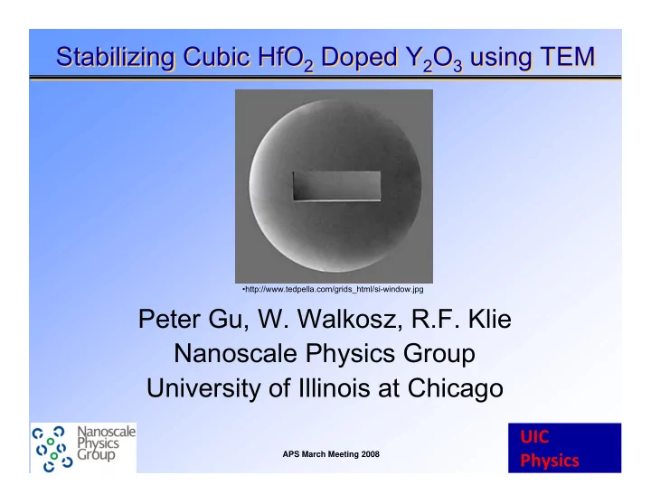
Stabilizing Cubic HfO 2 Doped Y 2 O 3 using TEM Stabilizing Cubic HfO 2 Doped Y 2 O 3 using TEM http://www.tedpella.com/grids_html/si-window.jpg Peter Gu, W. Walkosz, R.F. Klie Nanoscale Physics Group University of Illinois at Chicago UIC
Stabilizing Cubic HfO 2 Doped Y 2 O 3 using TEM Stabilizing Cubic HfO 2 Doped Y 2 O 3 using TEM •http://www.tedpella.com/grids_html/si-window.jpg Peter Gu, W. Walkosz, R.F. Klie Nanoscale Physics Group University of Illinois at Chicago UIC APS March Meeting 2008 Physics
Moore’s Law Moore’s Law • 1965 by Intel cofounder, Gordon Moore • Exponential increase in transistor density • Limit to trend • SiO 2 (2 nm – breakdown) • Criteria • Insulating • Thermally Stable • Chemically Stable • High κ materials •http://www.developers.net/storyImages/062404/inteldemystifying1.jpg UIC APS March Meeting 2008 Physics
XRD-data XRD-data GI-XRD 2.5% Y in HfO2 annealed at different temperatures 1000 900 800 monclinic-HfO2 (111) 700 (200) (220) (311) (222) 925 C Intensity 600 cubic-HfO2 800 C (101) 500 (211) (112) (110) (200) (002) (103) 400 tetra.-HfO2 600 C 300 200 100 0 10 20 30 40 50 60 70 2 Theta Image from professor Takoudis’ group UIC APS March Meeting 2008 Physics
XRD-data XRD-data GI-XRD 20% Y in HfO2 annealed at different temperatures 1000 900 800 monclinic-HfO2 700 (220) (311) (222) (200) (111) 925 C Intensity 600 800 C cubic-HfO2 500 (101) (112)(200) (103)(211) (002) (110) 400 tetra.-HfO2 600 C 300 200 100 0 10 20 30 40 50 60 70 2 Theta Image from professor Takoudis’ group UIC APS March Meeting 2008 Physics
κ vs Yttrium Concentration κ vs Yttrium Concentration % Yttrium • concentration measured via XPS κ measured via CV • Local Max ~ 20% • Yttrium •Image from professor Takoudis’ group UIC APS March Meeting 2008 Physics
Research Plan Research Plan • Samples: • Annealed 2.5% Y 2 O 3 on HfO 2 • Unannealed 2.5% Y 2 O 3 on HfO 2 • Annealed 20% Y 2 O 3 on HfO 2 • TEM 3010 • Diffraction mode • Check crystal structure – polymorphs (cubic vs. tetragonal vs. monoclinic) • Check for homogeneity • SiO 2 layer thickness • Grain Size •Journal of Applied Physics 103, 084103 (2008) UIC APS March Meeting 2008 Physics
2.5% Y 2 O 3 Un-Annealed 2.5% Y 2 O 3 Un-Annealed 2.5% Yttrium Oxide / Hafnium Oxide Un-Annealed Sample Image at 150,000 Magnification Silicon Substrate Silicon Dioxide Hafnia / Yttria film -layers Epoxy UIC APS March Meeting 2008 Physics
2.5% Y 2 O 3 Un-Annealed - Diffraction 2.5% Y 2 O 3 Un-Annealed - Diffraction 2.5% Yttrium Oxide / Hafnium Oxide Un-Annealed Sample Image at 50 cm Camera Length •Superimposed Patterns •Spot Pattern – Silicon Substrate (001) •Cubic structure •Fuzzy circular – Film •Amorphous UIC APS March Meeting 2008 Physics
2.5% Y 2 O 3 Annealed 2.5% Y 2 O 3 Annealed 2.5% Yttrium Oxide / Hafnium Oxide Annealed Sample Image at 600,000 Magnification Silicon Substrate Silicon Dioxide Hafnia / Yttria film Epoxy UIC APS March Meeting 2008 Physics
2.5% Y 2 O 3 Annealed - Diffraction 2.5% Y 2 O 3 Annealed - Diffraction 2.5% Yttrium Oxide / Hafnium Oxide Annealed Sample Image at 50 cm Camera Length •Superimposed Patterns •Spot Pattern – Silicon Substrate (001) •Cubic structure •Concentric Circular pattern– Film •Cubic Hafnium Oxide UIC APS March Meeting 2008 Physics
20% Y 2 O 3 Annealed 20% Y 2 O 3 Annealed 20% Yttrium Oxide / Hafnium Oxide Annealed Sample Image at 500,000 Magnification Epoxy Hafnia / Yttria film Silicon Dioxide Silicon Substrate UIC APS March Meeting 2008 Physics
20% Y 2 O 3 Annealed - Diffraction 20% Y 2 O 3 Annealed - Diffraction (3,1,-1) Si 20% Yttrium Oxide / (4,0,0) Si Hafnium (-1,3,-3) Si (0,2,-2) Si Oxide Annealed Sample (1,1,-1) Si (2,0,0)Si Image at 50 cm Camera •(3,-1,1) Si (-2,2,-2) Si Length (-1,1,-1) Si •Superimposed Patterns (0,0,0) Si (1,-1,1) Si •Spot Pattern – Silicon Substrate (001) (2,-2,2) Si (-3,1,-1) Si (1,1,1) HfO2 •Cubic structure (-2,0,0) Si •Concentric Circular (-1,-1,1) Si (2,0,0) HfO2 pattern– Film (0,-2,2) Si •Cubic Hafnium (1,-3,3) Si (-4,0,0) Si Oxide (1,1,3) HfO2 (-3,-1,1) Si (-2,-2,2) Si (-1,-3,3) Si (0,-4,4) Si (-5,-1,1) Si UIC (-4,-2,2) Si APS March Meeting 2008 Physics (-3,-3,3) Si
SiO 2 Layer Analysis SiO 2 Layer Analysis + film layer thickness SiO layer thickness film layer thickness SiO layer thickness = 2 2 + film dielectric constant SiO dielectric constant total dielectric constant 2 • Expected for 30 nm film thickness: • ~3 nm for 20% Y 2 O 3 • ~12 nm for 2.5% Y 2 O 3 • Silicon Dioxide Layer Analysis 2.5% Y 2 O 3 2.5% Y 2 O 3 20% Y 2 O 3 unannealed(nm) annealed(nm) annealed(nm) average 2.289 3.072 3.175 max 3.845 5.774 4.2 min 0.939 1.303 0.765 stdev 0.875 1.332 0.759 UIC APS March Meeting 2008 Physics
Grain Size Analysis Grain Size Analysis Grain Size Measurements - 20% Grain Size Measurements - 2.5% annealed sample annealed sample Along Grain Perpendicular to Grain Along Grain Perpendicular to Grain (nm) (nm) (nm) (nm) Average (nm) 4.339 5.510 5.705 5.069 Standard Dev. 0.833 1.217 1.007 1.507 UIC APS March Meeting 2008 Physics
Summary / Conclusion Summary / Conclusion • 20% Annealed Sample has a larger dielectric constant than 2.5% Annealed Sample • No Difference in Structural makeup of interfacial film (Both cubic polymorph) • No Difference in Silicon Dioxide Layer Thickness • No Difference in Grain Size • Difference in film shape or thickness? • Difference in Oxygen Concentration? UIC APS March Meeting 2008 Physics
Acknowledgements Acknowledgements • National Science Foundation • Grant NSF EEC 0755115 • NSF CMS 0829903 • Department of Defense • Professor R.F. Klie • Professor C. Takoudis • Professor G. Jursich • PhD G. Yang • PhD Q. Tao • Weronica Walkosz • Ke-Bin Low • K.C. Kragh UIC APS March Meeting 2008 Physics
References References 1. E. Rauwel, C. Dubourdieu, B. Hollander, N. Rochat, F. Ducroquet, M. D. Rossell, G. Van Tendeloo, • and B. Pelissier, Stabilization of the cubic phase of HfO 2 by Y addition in films grown by metal organic chemical vapor deposition, Appl. Phys. Lett. 89, 012902 (2006), DOI:10.1063/1.2216102 2. Muller, D, A sound barrier for silicon?, Nature Materials. 4, 9, 645 (2005) DOI:10.1038/nmat1466 • 3. Milgrom, Lionel, Hafnium oxide helps make chips smaller and faster, RSC Chemistry World. (2007) • 4. Z. K. Yang, W. C. Lee, Y. J. Lee, P. Chang, M. L. Huang, M. Hong, K. L. Yu, M.-T. Tang, B.-H. Lin, C.- • H. Hsu, and J. Kwo, Structural and compositional investigation of yttrium-doped HfO 2 films epitaxially grown on Si (111), Appl. Phys. Lett. 91, 202909 (2007), DOI:10.1063/1.2816121 5. Eric Cockayne, Effect of ionic substitutions on the structure and dielectric properties of hafnia: A first • principles study, J. Appl. Phys. 103, 084103 (2008), DOI:10.1063/1.2903870 6. Koji Kita, Kentaro Kyuno, and Akira Toriumi, Permittivity increase of yttrium-doped HfO[sub 2] through • structural phase transformation, Appl. Phys. Lett. 86, 102906 (2005), DOI:10.1063/1.1880436 7. Smith, D.J.; Vetelino, J.F.; Falconer, R.S.; Wittman, E.L., "Stability, sensitivity and selectivity of • tungsten trioxide films for gas sensing applications," Solid-State Sensor and Actuator Workshop, 1992. 5th Technical Digest., IEEE , vol., no., pp.78-81, 22-25 Jun 1992 8. J.P. Salerno, “Single Crystal Silicon AMLCDs”, Conference Record of the 1994 International Display • Research Conference (IDRC), pp. 39-44, 1994. 9. B. Škipina, T. Č ajkovski, M. Davidovi ć , D. Č ajkovski, V. Likar-Smiljani ć and U. B. Mio č , “Conductivity of • Grains and Grain Boundaries in Polycrystalline Heteropoly Acid Salts,” Materials Science Forum, 2005, 494, 101-106 10. Takoudis et al. private communications • 11. M. Agarwal, M. R. DeGuire, and A. H. Heuer, Synthesis of yttrium oxide thin films with and without • the use of organic self-assembled monolayers, Appl. Phys. Lett. 71, 891 (1997), DOI:10.1063/1.119679 12. J.M. Zuo and J.C. Mabon, Web-based Electron Microscopy Application Software: Web-EMAPS, • Microsc Microanal 10(Suppl 2), 2004; URL: http://emaps.mrl.uiuc.edu/ UIC APS March Meeting 2008 Physics
Recommend
More recommend
Explore More Topics
Stay informed with curated content and fresh updates.
