St Stress Aware Layout Stress Aware Layout St A A L L t t - PowerPoint PPT Presentation
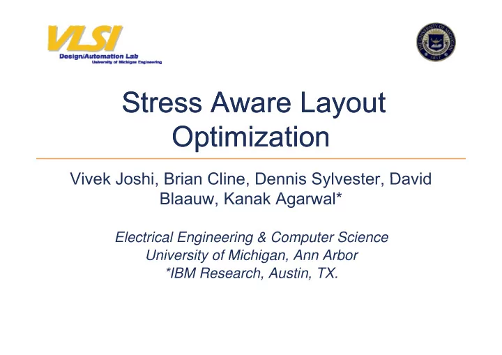
1 St Stress Aware Layout Stress Aware Layout St A A L L t t Optimization Optimization Optimization Optimization Vivek Joshi Brian Cline Dennis Sylvester David Vivek Joshi, Brian Cline, Dennis Sylvester, David Blaauw, Kanak Agarwal*
1 St Stress Aware Layout Stress Aware Layout St A A L L t t Optimization Optimization Optimization Optimization Vivek Joshi Brian Cline Dennis Sylvester David Vivek Joshi, Brian Cline, Dennis Sylvester, David Blaauw, Kanak Agarwal* Electrical Engineering & Computer Science University of Michigan Ann Arbor University of Michigan, Ann Arbor *IBM Research, Austin, TX. 1
Outline 2 � Introduction & motivation � Simulation at device level � Guidelines to improve performance via layout � Applying guidelines to standard cell layouts � Applying guidelines to standard cell layouts � Conclusions and future work 2 University of Michigan
Introduction 3 � Maintaining performance and reliability with scaling is difficult � Can no longer scale tox, VDD, V th as aggressively as L � Mobility degradation due to higher effective fields M bilit d d ti d t hi h ff ti fi ld � Introduce mechanical stress in channel to enhance carrier transport transport � Alters valence and conduction bands � Changes effective carrier mass and/or band scattering rates � Increase in carrier mobility results in higher performance and leakage 3 University of Michigan
Introduction 4 � NMOS and PMOS have different desired stress in different Gate Si Depth Later directions Gate Source Drain Source Source Drain Drain ral � Stress generated due to thermal Longitudinal and lattice mismatch d l tti i t h NMOS PMOS Longitudinal Tensile Compressive � Four main sources of stress � Four main sources of stress Lateral Lateral Tensile Tensile Tensile Tensile Si Depth Compressive Tensile � Shallow trench isolation � Embedded SiGe T – Tensile Nitride Liner T Tensile Nitride Liner � Dual-stress nitride liner C – Compressive Nitride C T � Stress memorization technique Liner eSiGe eSiGe STI NMOS PMOS PMOS 4 University of Michigan
Dependence of Channel Stress on Layout 5 � Amount of stress transferred has a strong dependence on layout � Longer active area (higher L s/d ) – g ( g s/d ) more SiGe, STI pushed away � Contacts away from channel – more L s/d L s/d stress due to nitride, no contacts - stress due to nitride, no contacts higher stress � SMT – uniform, not considered in this analysis analysis Nitride Liner Nitride Liner Nitride Liner Nitride Liner SiGe SiGe SiGe SiGe STI STI STI STI � Two devices with same W, L can Silicon Silicon differ significantly in performance � We study this dependence and � We study this dependence and L s/d suggest layout guidelines to enhance channel stress 5 University of Michigan
Previous Work 6 � Focus on modeling stress due to various sources F d li t d t i � No comprehensive model that considers all layout dependent N h i d l th t id ll l t d d t sources � Extensive research and modeling focused on STI � Accurate device level modeling (included in BSIM4) Accurate device level modeling (included in BSIM4) � Efficient white-space management placement algorithms � BUT: Contribution of STI to stress induced in channel is minor compared to other sources compared to other sources � No research has focused on new standard cell library design No research has focused on new standard cell library design exploiting stress, while considering all layout dependent sources 6 University of Michigan
Comparison to V th reduction 7 � Mobility enhancement - � Saturation current – sub-linear dependence dependence � Leakage current – linear � V th reduction V th reduction � Saturation current – almost linear � Leakage current – exponential g p Stress Based Stress Based � Mobility enhancement shows a 1.18 V th Based 1.16 better tradeoff 1.14 d) 1 12 1.12 n (normalized � In 65nm, stressed PMOS 1.10 achieves 12% Ion improvement 1.08 with ½ leakage penalty of V th with ~½ leakage penalty of V th 1.06 Ion 1.04 reduction 1.02 1.00 0 0 1 1 2 2 3 3 4 4 5 5 6 6 7 7 8 8 9 10 11 12 13 14 15 16 9 10 11 12 13 14 15 16 Ioff (normalized) 7 University of Michigan
Simulation Flow 8 � Tsuprem4 for simulating device fabrication � Stress values imported into St l i t d i t Davinci � solves stress- based equations based equations Simulated Stress in Simulated Stress in Simulating Device Simulating Device Fabrication in Tsuprem4 the Channel � Resulting drain currents consistent with published consistent with published results [IBM65, IEDM05] � Based on simulation, analyze Based on simulation, analyze I off I on I I off I on I layout dependencies to develop guidelines I on Ioff Layout Parameter Layout Parameter Layout Parameter Layout Parameter Dependence on Layout epe de ce o ayout Parameters using Davinci 3D TCAD Tool 8 University of Michigan
Simulation for Isolated Device - PMOS 9 � Vary source/drain length (L s/d ) � 12% performance increase 1 1 for 3.8X increase in leakage f 3 8X i i l k Drive Current � Superior tradeoff to Vth Leakage 8 reduction reduction 1.16 1.14 � Leakage tradeoff better for lower 6 1.12 power libraries ed) Ioff 1.10 on (normalize f (normalized � Ion gains saturate beyond L s/d 4 1.08 of 1.6 1.58 1.06 Io d) � Ion gains sensitive to contact 1.04 1 04 2 1.02 placement 1.00 0 � 2.6% of improvement % f 1.0 1.2 1.4 1.6 1.8 2.0 L s/d (normalized) � No contact – 4% higher Ion 9 University of Michigan
Simulation for Isolated Device - NMOS 10 � 5% performance increase for 1.5X leakage increase Drive Current 1 Leakage � Less sensitive than PMOS 1.7 1.06 � Increasing only longitudinal 1.6 1.05 nitride stress Ioff (norm malized) 1.5 1.04 � Moving away STI, not as Moving away STI, not as 1.4 Ion (norm malized) 1.03 effective as eSiGe increase 1.3 1.02 1.2 1.1 1.01 1.01 � Contact placement becomes 1.58 1.0 1.00 more important 0.9 1.0 1.2 1.4 1.6 1.8 2.0 � No contact – 2% higher Ion L L s/d (normalized) ( li d) 10 University of Michigan
Layout Guideline 1 11 “ Increase the active area in a given cell to fill up the entire “ Increase the active area in a given cell to fill up the entire cell width while obeying DRC rules” � Most readily applied to compact pull-up and pull-down Most readily applied to compact pull up and pull down networks � Ex: PMOS stack in NOR, NMOS in NAND � Increases S/D capacitance – apply to cells with larger output loading � Can apply to cells to create slightly larger high performance C l ll li h l l hi h f versions Cell Boundary Cell Boundary Cell Boundary Cell Boundary PMOS Stack 11 University of Michigan
Layout Guideline 2 12 “ Move contacts away from gate polysilicon as much as possible” � Nitride transfers stress in two ways: vertically through the Nit id t f t i t ti ll th h th gate, longitudinally � Increases longitudinal component I l it di l t � Limited improvement – due to increasing only one component � Increases S/D resistance - typically very small increase (<5 Ω ) T – Tensile Nitride Liner T Tensile Nitride Liner C – Compressive Nitride C T Liner eSiGe eSiGe STI NMOS PMOS PMOS 12 University of Michigan
Layout Guideline 3 13 “ In the lateral direction, move PMOS closer to tensile/compressive nitride interface and NMOS away from it” from it � Curious behavior at interface – compressive stress under tensile nitride and vice versa tensile nitride and vice versa � Both NMOS and PMOS need tensile stress in this direction � Space readily available for transistors with smaller widths � Space readily available for transistors with smaller widths � Ex: X1 variants of various gates COMPRESSIVE NITRIDE TENSILE NITRIDE POLY STI SILICON 13 University of Michigan
Position Dependence of Stress 14 � “Center” devices in denser layouts have higher channel stress � NMOS: STI pushed away � PMOS: more eSiGe, more stress, as SiGe has higher contribution as compared to STI � Can result in design issues, noise margin degradation, speed issues for certain dynamic circuits, etc. 1 1 2 2 3 3 D E V IC E 1 D E V IC E 1 D E V IC E 2 D E V IC E 2 D E V IC E 3 D E V IC E 3 14 University of Michigan
Applying guidelines to a 3 Input NOR 15 � Apply guideline 1 - ~22% increase in PMOS active area � Apply guideline 2 – Move contacts 1,2 1,2 away from PMOS after increasing f PMOS ft i i active area 3 � Apply guideline 3 – move PMOS and NMOS as shown and NMOS as shown 3 � Drive current enhancement � Drive current enhancement - ~13.5% for PMOS, ~3% for NMOS 15 University of Michigan
Applying guidelines to a 3 Input NAND 16 � Apply guideline 1 - ~20% increase in NMOS active area � Apply guideline 2 – Move A l id li 2 M contacts away from NMOS after increasing active area increasing active area � Apply guideline 3 – move PMOS 3 and NMOS as shown and NMOS as shown � Drive current enhancement - 1,2 1,2 ~1.5% for PMOS, ~7% for NMOS 1.5% for PMOS, 7% for NMOS � Lower improvements because 3 nitride transfers stress vertically y and longitudinally 16 University of Michigan
Recommend
More recommend
Explore More Topics
Stay informed with curated content and fresh updates.
