Quantum transport measurements on Bi 2 Se 3 topological insulators - PowerPoint PPT Presentation
Quantum transport measurements on Bi 2 Se 3 topological insulators Jrn Wilhelm 26.11.2012 Motivation Spintronic = Spin based electronics Classical Spintronic Use of electron spin in conventional hard disks GMR Giant
Quantum transport measurements on Bi 2 Se 3 topological insulators Jörn Wilhelm 26.11.2012
Motivation Spintronic = Spin based electronics • „Classical“ Spintronic • Use of electron spin in conventional hard disks • GMR – Giant Magneto Resistance effect Conventional Hard disk [CHJ] • „Modern“ Spintronic • Spin currents • Spin transistor Spin Field Effect transistor [IHT]
Introduction “Insulator” : Band gap between valence- and conduction band “Topological“ : Conducting spin-split 1D (2D) edge states within the band gap Topological Insulators are conducting! Simple band structure [HK10]
Topological Insulators Analogy: Quantum Spin Hall Effect ≈ superposition of 2 counter-orientated QHE Topological Insulator : „Internal“ magnetic field caused by spin-orbit interaction!
Band structure Bi 2 Se 3 Spin-orbit interaction causes band inversion at the Brillouin zone center Γ Valence- and conduction band at Γ Ab initio calculations of Bi 2 Se 3 including following effects: surface states [SZ09] (I) Chemical bonding (II) Crystal field distortion (III) Spin-orbit coupling [SZ09]
Bi 2 Se 3 ARPES measurements 2009 ARPES measurements: Bi 2 Se 3 is topological insulator! BUT! Destinct topological properties not useable! ARPES data Bi 2 Se 3 2009 [HH09] Goal: • Preparation of non (bulk) conducting Bi 2 Se 3 crystals • Quantum transport measurements on surface states W 𝐢𝐢 𝐂𝐂 𝟑 𝐓𝐓 𝟒 ? • Large 𝐹 – Room temperature spintronic applications
Crystal structure Bi 2 Se 3 Problems: Causes: n-type doping by crystal defects • Se vacancies (+2 e-) • Bad growth start cause layer of poor crystal quality (a) Unit cell Bi 2 Se 3 (b) On top view (c) Cross section TEM substrate interface [TM12] [SZ09]
Sample preparation and layout Lithography process diagram Top-view without gate Sample bonded to carrier Preparation and layout: • Made from Bi 2 Se 3 (Si/InP substrate) Wafer piece • Sample preparation by means of photolithography • 2 Hall bar layout (600 x 200) 𝜈𝑛 und (10 x 30) 𝜈𝑛
Transport setup Setup: p: 4 He − cryostat • • T = 4.2 K • Superconducting magnet • B ⊥ − field up to 14 T • DC – measurements Circuit diagram [MR11] “14T”- Setup Ep3 Wuerzburg
Samples on Silicon substrate Samples on Silicon : • High densities • Low mobilities • Bulk conductance Lattice constants: 𝑏 𝑇𝑇 ( 111 ) = 3.84 Å • 7% 𝑏 𝐶𝑇 2 𝑇𝑇 3 ( 111 ) = 4.14 Å • 𝑏 𝐽𝐽𝐽 ( 111 ) = 4.15 Å • InP substrate
Samples on InP + Fe, annealed Samples on InP : • Lower densities • Higher mobilities • Non linear Hall • 2 different carriers Large domains visible in AFM images High sample quality
High field measurements The Bi 2 Se 3 thickness of 190 nm is >> 2D system, therefore: If Quantum Hall Effect • 2D System • Conduction via surface states • Topological insulator Bitter-magnet HMFL Nijmegen
Magnetic field rotation True 2D electron gas: • Oscillations independent of B || component! • Oscillations periodic in 1/B • Only holds up to 50 𝑝 • Oscillations only in some cases periodic in 1/B • Oscillations caused by other effects? • Multiple oscillation frequencies?
Summary Goals: • Growth of bulk insulating Bi 2 Se 3 • Quantum transport measurements of 3D TI surface states Results: • Improvement of carrier density and carrier mobility • Established growth on InP substrates • High field measurements: Surface states or bulk oscillations (!?)
Thank you for your kind attention!
Sources [HK10] Z. Hasan, L. Kane. Colloquium: Topological Insulators, Review of modern physics, vol. 82, 2010 [SZ09] S. C. Zhang et al. Topological insulators in Bi2Se3, Bi2Te3 and Sb2Te3 with a single Dirac cone on the surface . Nature Physics, 5:438, 2009. [MR11] M. Reuß. Transporteigenschaften dreidimensionaler topologischer Isolatoren , Diplomarbeit, Physikalische Fakultät Universität Würzburg, 2011. [HH09] M. Hasan, D. Hsieh et al. A tunable topological insulator in the spin helical Dirac transport regime, Nature vol. 460, 2009 [TM12] N. Tarakina, L. Molenkamp et al. Comparative Study of the Microstructure of Bi2Se3 Thin Films Grown on Si(111) and InP(111) Substrates, Crystal Growth and Design, 2012 [CHJ] C. Jansky, public domain, wikipedia.org/festplatte. [IHT] Institut für Halbleitertechnik, Universität Köln, iht.uni-stuttgart.de/forschung/spinplasm
Band structure Bi 2 Se 3 Ab initio band simulations: (a) without SOC (b) with SOC
Topological Insulators Time reversal symmetry maintained since B 𝑈𝑝𝑈𝑈 = 0 ! [HK10] 3D: ( − 1) 𝑤0 = ∏ 8 Γ 𝑇 : Kramers degenerate points 𝜀 ( Γ 𝑇 ) [HK10] 𝑇=1 (a) No topological insulator at even number of intersections (b) ℤ 2 topological insulator at Δ𝜑 0 = 𝑂𝑛𝑂𝑂𝑂 = 1
Photolithography Lithography process diagram
Transport measurements 1 Carrier model: 𝐵 𝐼 = 1 𝑜 = 1 𝐽 𝐶 = 1 𝐶 𝜈 = 𝜏 𝑚 𝑆 𝐼 𝑜𝑓 = 𝑜𝑜 𝐶 𝑓𝑂 𝑉 𝐼 𝑓𝑂 𝑆 𝐼 𝑆 𝑦𝑦 𝑐 2 Carrier model: 2 𝑜 1 + 𝜈 2 2 𝑜 2 + 𝜈 1 𝜈 2 𝐶 2 ( 𝑜 1 + 𝑜 2 ) 𝜈 1 𝐵 𝐼 = ∓𝑓 −1 ( 𝜈 1 | 𝑜 1 | + | 𝑜 2 |) 2 + 𝜈 1 𝜈 2 𝐶 2 ( 𝑜 1 + 𝑜 2 ) 2 • Determination of transport parameters via Hall measurements • Fit 1 or 2 carrier model to data
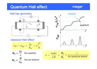
Topological Insulators Quantum Hall Effect: Laughlin Picture: 𝜁 𝑛 = ℏ𝜕 𝑑 m + 1 𝑂 𝜏 𝑦𝑦 = 𝑂 𝑓 2 ℎ Hall constant can be calculated From the Berry flux 𝑂 = � 𝑜 𝑛 [SG10] 𝑛 𝑉 = 𝑜 𝑓 2 𝐽 = Δ𝐺 ΔΦ = 𝑜𝑓 ( 𝜈 − 𝜈 𝑇 ) 𝐻 = 𝐽 𝑜 𝑛 = � 𝑂 2 𝒍 ( 𝛼 × (i ⟨𝑣 𝑛 | 𝛼 𝑙 | 𝑣 𝑛 ⟩ )) ℎ ℎ
Samples on ZnCdSe buffer Samples with ZnCdSe buffer: • Better densities • Higher mobilities Draw backs: • Difficult growth • New error types
Samples on InP + Fe, miscut Iron doped InP substrate: • InP insulating • Better carrier densities • Higher mobilities (compared to Si(111)) Miscut: • Surface miscut relative to InP(111) • Idea: stepwise growth [TM12]
Fourier transformation 2 frequencies = 2 surface states ? • Hard to get carrier densities from few oscillations • Signal to weak for FFT
Temperature dependence
Recommend
More recommend
Explore More Topics
Stay informed with curated content and fresh updates.
