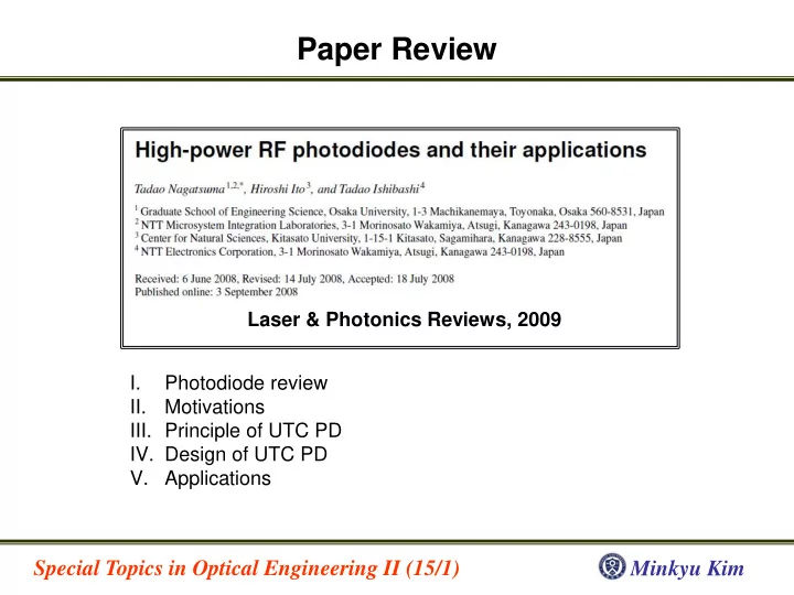
Paper Review Laser & Photonics Reviews, 2009 I. Photodiode - PowerPoint PPT Presentation
Paper Review Laser & Photonics Reviews, 2009 I. Photodiode review II. Motivations III. Principle of UTC PD IV. Design of UTC PD V. Applications Special Topics in Optical Engineering II (15/1) Minkyu Kim Photodetection
Paper Review Laser & Photonics Reviews, 2009 I. Photodiode review II. Motivations III. Principle of UTC PD IV. Design of UTC PD V. Applications Special Topics in Optical Engineering II (15/1) Minkyu Kim
Photodetection • Photodetection -Produces current when ℎ𝜉 > 𝐹 -Different absorption coefficient with different material( 𝐹 ) 𝐽 -R(Responsivity) = 𝑄 Special Topics in Optical Engineering II (15/1) Minkyu Kim
Phototectors Photoconductor PN junction photodiode PIN junction photodiode ℎ𝜉 • • • Easy to make Reverse bias Reverse bias • • • Slow Small dark current Solve efficiency problem • • Dark current Drift in depletion region of PN junction PD • Thin depletion region bad efficiency Special Topics in Optical Engineering II (15/1) Minkyu Kim
Demands for High Power RF PD • Power amp can be followed by PD Only when amplifier is available at frequencies of interest • High frequency optical signals High speed PD required Special Topics in Optical Engineering II (15/1) Minkyu Kim
Principle of UTC PD (a) UTC PD (b) PIN PD * UTC : Uni Traveling Carrier • Light absorption layer(p-type) + Carrier collection layer(transparent) • Generated hole respond very quickly within in the dielectric relaxation time • Generated electron exhibit velocity overshoot in carrier collection layer (Condition : quasi-field in the absorption layer by doping grading, bias for overshoot velocity) • Electron diffusion time mainly determines the operation speed Special Topics in Optical Engineering II (15/1) Minkyu Kim
Pulse Response (a) UTC PD (b) PIN PD • Current tails observed due to the slow response of holes in PIN PD • No current tails in UTC PD due to the fast response of holes Special Topics in Optical Engineering II (15/1) Minkyu Kim
Bandwidth • Conventional PIN PD -Trade-off between transit time vs RC time 𝑈𝑠𝑏𝑜𝑡𝑗𝑢 𝑢𝑗𝑛𝑓 𝑚𝑗𝑛𝑗𝑢𝑓𝑒 𝐶𝑋 ∝ 1 𝑒 𝑆𝐷 𝑢𝑗𝑛𝑓 𝑚𝑗𝑛𝑗𝑢𝑓𝑒 𝐶𝑋 ∝ 1 𝑆𝐷 ∝ 𝑒 𝑒 : Thickness of absorption layer • UTC PD -No trade-off in thickness of layer due to diffusive electron transport in absorption layer Thinner absorption layer increases BW Special Topics in Optical Engineering II (15/1) Minkyu Kim
Output Saturation Current (a) UTC PD (b) PIN PD • Photogenerated carriers(electron & hole) are stored in the absorption layer in conventional PIN PD Decrease E field Current saturation • Only electrons whose velocity at overshoot stored in UTC PD Current saturation occurs at much higher intensity Special Topics in Optical Engineering II (15/1) Minkyu Kim
Structure Design Distributed Waveguide(WG) PD Refracting Facet(RF) PD Surface(vertical) illuminated PD Waveguide-fed Waveguide(WG) PD evanescently coupled PD Distributed Waveguide-fed evanescently coupled PD Improve responsivity while maintaining BW Improve responsivity & BW Special Topics in Optical Engineering II (15/1) Minkyu Kim
Circuit Design • Integration with a short-stub matching circuit Increase output power, bandwidth Special Topics in Optical Engineering II (15/1) Minkyu Kim
Applications • High-speed wireless communications - Promising technique for “uncompressed” HDTC broadcasting -UTC PD can make transmitter core very compact and light-weight Schematic diagram of wireless link • Spectroscopic measurement systems -Using photonic LO is best combination due to low noise Experiment setup for spectroscopic system Special Topics in Optical Engineering II (15/1) Minkyu Kim
Conclusion • High power RF photodetector required in microwave photonics • UTC PD -Larger bandwidth -Higher saturation current -Better pulse response • Structure & circuit design Improvement of responsivity & bandwidth • Microwave photonics applications Special Topics in Optical Engineering II (15/1) Minkyu Kim
Recommend
More recommend
Explore More Topics
Stay informed with curated content and fresh updates.


