Optimality of Packing Shigetoshi Nakatake Univ. of Kitakyushu 1 - PowerPoint PPT Presentation
ISPD 2013 Commemoration for Professor Y. Kajitani Practicality on Placement Given by Optimality of Packing Shigetoshi Nakatake Univ. of Kitakyushu 1 Commemoration for Professor Y. Kajitani : ISPD 2013 Todays Talk 1) Rect. packing-base
ISPD 2013 Commemoration for Professor Y. Kajitani Practicality on Placement Given by Optimality of Packing Shigetoshi Nakatake Univ. of Kitakyushu 1 Commemoration for Professor Y. Kajitani : ISPD 2013
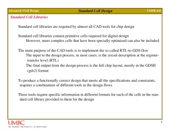
Today’s Talk 1) Rect. packing-base analog placement Sequence-pair Packing Constraint-driven Optimization 2) With or without packing scenario, how do we develop analog placement? Analytical Analog placement with proximity constraints Comparison : w/ and w/o topological packing technique 2 Commemoration for Professor Y. Kajitani : ISPD 2013
2D Rect. Packing INPUT: A set of rectangles, each of which has width and height OUTPUT: A placement of rectangles SUBJECT TO: No overlapping of any pair of rectangles OBJECTIVE: Minimize bounding box of all the rectangles Sequence-Pair[ICCAD95], [TCAD96] 3 Commemoration for Professor Y. Kajitani : ISPD 2013
Topological Representation and Constraint Graphs Placement Constraint graphs: (w/o any overlapping): b b w(b)/2 a c h(a)/2 c a a w(a)/2 b vertical const. graph horizontal const. graph NOTE: Gv, Gh are weighted DAG Topological description: Compacted placement: a is left-of c (c is right of a) a b is left-of c (c is right of b) b is below a (a is above b) c b 4 Commemoration for Professor Y. Kajitani : ISPD 2013
Sequence-Pair(1) Placement Sequence-Pair ( , ) ( abcdef, bfcaed ) SP d a a d c e e b c bf caed a b cdef b f f Oblique-Line-Grid: Equivalent Representation of SP 1 X : position of X in 1 1 1 1 ( ) ( ) ( ), ( ) ( ) X Y X Y X is left-of Y 1 X 1 1 1 1 ( ) ( ) ( ), ( ) ( ) : position of X in X Y X Y X is below Y 5 Commemoration for Professor Y. Kajitani : ISPD 2013
Sequence-Pair(2) Gh: horizontal constraint graph Gv: vertical constraint graph T v a d a d S c e T h h b c e b f f S Y v X Y w(X)/2+w(Y)/2 h(X)/2+h(Y)/2 X NOTE: w(X) , h(X): width, height of X 6 Commemoration for Professor Y. Kajitani : ISPD 2013
Sequence-Pair(3) 1. Every placement corresponds to a sequence-pair 2. Packing according to constraint graphs can generate a minimal area placement under the same topological description 3. A solution space induced by sequence- pairs always includes an optimum placement with respect to area 7 Commemoration for Professor Y. Kajitani : ISPD 2013
Sequence-Pair(4) Application to simulated annealing Moves: 1. FullExchange(a,b): a b b a a b b a b a a b and pair-exchange on both | 2. HalfExchange(a,b, ): b a a b a b a b a a b b b a a b a b a a b a b b pair-exchange on pair-exchange on 8 Commemoration for Professor Y. Kajitani : ISPD 2013
Practical Applications of Packing • Building block placement • Floorplanning for large scale circuits • Analog placement • 3D Cube packing • Polygon packing • Scheduling for dynamic reconfigurable system … 9 Commemoration for Professor Y. Kajitani : ISPD 2013
Analog Placement Device Generation Cell Design Block Design Each Placement… 1. Circuit netlist ? Layout 2. Design rule (Layers w/ Geometry, 3. Specification / Contacts, Wires…) constraints 10 Commemoration for Professor Y. Kajitani : ISPD 2013
Analog Placement • Geometry-based placement – ILAC [CICC88], KOAN/ANAGRAM [ICCAD88] larger area and time consuming • Topology-based placement (modern) – BSG, Sequence-Pair, O-tree, B*-tree, TCG-S, … – Constraint-driven • symmetry, common-centroid, alignment and others smaller area and rapid convergence 11 Commemoration for Professor Y. Kajitani : ISPD 2013
Constraint-driven Placement 1. Formulation as a rectangle packing problem 2. Extensions under constraints Separation Constraint Alignment Constraint Abutment Constraint Boundary Constraint Symmetry Constraint symm-const. Preplaced Constraint Range Constraint Cluster Constraint cluster-const. 12 Commemoration for Professor Y. Kajitani : ISPD 2013
Our Works in Constraint-driven Analog Layout • Placement – ASPDAC04, GLSVLSI04, IEICE04, ISVLIS06a, ASPDAC09, ASPDAC08 – AMPER produced by JEDAT • Routing – GLSVLSI05, IEICE06 • Compaction – ASPDAC02, ISVLSI06b – GRANA produced by JEDAT [ICCAD95] H.Murata, K.Fujiyoshi, S. Nakatake, Y.Kajitani, “ Rectangle-Packing Based on Module Placement ”, ICCAD95, pp.472 -479, 1995. [TCAD96] VLSI H.Murata, K.Fujiyoshi, S.Nakatake, Y.Kajitani, “ Module Placement Based on Rectangle-Packing by the Sequence-Pair ”, IEEE Trans. on CAD, vol.15, No.12, pp.1518-1524, 1996. [ASPDAC02] Y.Kubo, S.Nakatake, Y.Kajitani, M.Kawakita, “ Explicit Expression and Simultaneous Optimization of Placement and Routing for Analog IC Layouts ”, ASPDAC02, pp.467 -472, 2002. [ASPDAC04] T.Nojima, X.Zhu, Y.Takashima, S.Nakatake, Y.Kajitani, “ Multi-Level Placement with Circuit Schema Based Clustering in Analog IC Layouts ”, ASPDAC04, pp.406 -411, 2004. [GLSVLSI04] T.Nojima, X.Zhu, Y.Takashima, S.Nakatake, Y.Kajitani, “ A Device-Level Placement with Multi-Directional Convex Clustering ”, GLSVLSI04, pp.196-201, 2004. [IEICE04] T.Nojima, X.Zhu, Y.Takashima, S.Nakatake, Y.Kajitani, “ A Device-Level Placement with Schema Based Clusters in Analog IC Layouts ”, IEICE Trans. on Fundamentals, Vol.E87 -A, No.12, pp.3301-3308, 2004. [IEICE06] N. Fu, S. Nakatake, Y. Takashima, Y. Kajitani, “ The Oct-Touched Tile: A New Architecture for Shape-Based Routing ” , IEICE Trans. on Fundamentals, Vol.E89-A, No.2, pp.448-445, 2006 . [ISVLSI06a] N Fu, S. Nakatake, M. Mineshima, “Multi -SP: A Representation with United Rectangles for Analog Placement and Routing ”, ISVLSI06, pp.38-43, 2006. [ISVLSI06b] T.Nojima, S.Nakatake, T.Fujimura, K.Okazaki, Y.Kajitani, N.Ono, “Adaptive Porting of Analog IPs with Reusable Con servative Properties”, ISVLSI06, pp.18 -23, 2006. [ASPDAC07] S.Nakatake, “Structured Placement with Topological Regularity Evaluation”, ASPDAC07, pp.215 -220, 2007. [ASPDAC08] Q.Dong, S.Nakatake, “Constraint - Free Analog Placement with Topological Symmetry Structure”, ASPDAC08, pp.186 -191, 2008. 13 Commemoration for Professor Y. Kajitani : ISPD 2013
Analog Constraint Formulation 14 Commemoration for Professor Y. Kajitani : ISPD 2013
Objective and Optimization • Objective: Area + Wirelength (HPWL or MST) • Framework: Simulated Annealing – Moves – Feasibility Check • Topological Checking sequence-pair conditions • Geometrical Checking no positive cycle 15 Commemoration for Professor Y. Kajitani : ISPD 2013
Design Flow for Analog Layout Schematic Entry Simulation & Netlist Generation Device Sizing Device Generation Layout Constraint Generation Constraint-Driven Placement Compaction Routing (option) LPE & PostLayout DRC, LVS Simulation 16 16 Commemoration for Professor Y. Kajitani : ISPD 2013
Design Case Study: LCD-Driver Level-Shifter BGR AMP BIAS manual const-driven const-driven manual const-driven manual NOTE: Both ICs by ‘ manual’ and ‘ const- driven’ implemented on NECEL 0.35um, both of them could work. (Collaboration with NEC micro systems.) manual const-driven 17 Commemoration for Professor Y. Kajitani : ISPD 2013
Today’s Talk 1) Rect. packing-base analog placement Sequence-pair Packing Constraint-driven Optimization 2) With or without packing scenario, how do we develop analog placement? Analytical Analog placement with proximity constraints Comparison : w/ and w/o topological packing technique 18 Commemoration for Professor Y. Kajitani : ISPD 2013
Representation of Placement (1) A B A B A B C C C (1) Schematic (2) Symbolic/Topological Placement (3) Physical/Geometrical Placement A B C (4) Electrical Placement 19 Commemoration for Professor Y. Kajitani : ISPD 2013
Representation of Placement (2) A B A B A B A B C C C C Schematic Topological Placement Geometrical Placement Electrical Placement Outputs Outline Layers I/O pin Parasitics Design rules Device size Device Layout(Place Device Floorpl Steps Generati ment/Routing/ LPE sizing anning on (PDK) Compaction) 20 Commemoration for Professor Y. Kajitani : ISPD 2013
Optimization of Placement Sensitivity-driven Constraint-driven A B A B (( )) (( )) C C X (( )) 1. Spec.: Voff < 1mV 1. Spec.: Voff < 1mV 2. Extract diff. pair (A, B) Input is up to here 3. Symm. Const.: A and B is x- 2. Generate parasitic network symmetry for X Input is up to here 3. Sensitivity analysis V V V 4. Represent placement and offset offset offset min( ) X X X constraint topologically A B C 4. Perturb placement of A, B, C 5. Search optimal placement and optimize placement under constraints 21 Commemoration for Professor Y. Kajitani : ISPD 2013
Recommend
More recommend
Explore More Topics
Stay informed with curated content and fresh updates.

