non-von Neumann computing? Abu Sebastian IBM Research Zurich - PowerPoint PPT Presentation
Computational memory: A stepping stone to non-von Neumann computing? Abu Sebastian IBM Research Zurich Stanford EE380, 7 th March 2018 IBM Research - Zurich Abu Sebastian, IBM Research - Zurich 2 IBM Research - Zurich Abu Sebastian, IBM
Computational memory: A stepping stone to non-von Neumann computing? Abu Sebastian IBM Research – Zurich Stanford EE380, 7 th March 2018
IBM Research - Zurich Abu Sebastian, IBM Research - Zurich 2
IBM Research - Zurich Abu Sebastian, IBM Research - Zurich 3
Outline Motivation for in-memory computing Constituent elements of computational memory Computational memory: Logical operations Computational memory: Arithmetic operations Computational memory: Computing with device dynamics Mixed-precision in-memory computing Summary & Outlook Abu Sebastian, IBM Research - Zurich 4
Abu Sebastian, IBM Research - Zurich 5
Internet of Things (IoT) 30B Internet of An estimated 30 billion 35% CAGR Things internet-connected devices by 2020 Billions of Devices And that the amount of data produced will be over 40 trillion gigabytes Connected Cars Wearables Connected / Smart TVs Tablets Smartphones Personal Computers 0B 2013 2020 Source : BI Intelligence Estimates Abu Sebastian, IBM Research - Zurich 6
The AI revolution Artificial Intelligence Information and Telecommunications Powered by Data Oil, Automobiles and Mass Production Steel, Electricity and Heavy Engineering Steam and Railways The Industrial Revolution Today 1700 Abu Sebastian, IBM Research - Zurich 7
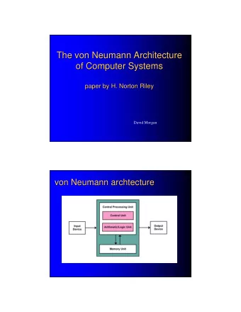
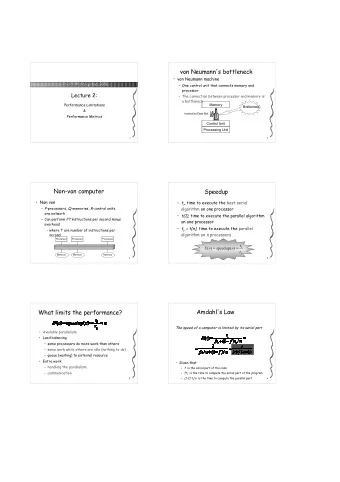
The computing challenge ~20W ~80,000 W 2880 processor threads 16 terabytes of RAM 80 kW of power 20 tons of air-conditioned cooling capacity Conventional von Neumann computing architecture IBM’s Watson in Jeopardy! MEMORY Input data Results CPU Abu Sebastian, IBM Research - Zurich 8
The computing challenge Landscape of AI Algorithms Largely CPUs Cognitive / AI “Human intelligence” exhibited by machines CPUs, FPGAs, GPUs Machine Advanced Analytics: Learning GPUs to train; NoSQL, Learning without explicit programming Hadoop & CPUs, FPGAs to inference; Analytics Race to ASICs Deep Learning Many-layer neural networks WEEKs to train certain deep neural networks! Abu Sebastian, IBM Research - Zurich 9
Advances in von Neumann computing Processor-in-memory Storage class memory Monolithic 3D integration (near memory computing) Access time Non-volatile Hard ~5 ms disk Slow STORAGE Flash MEMORY ~100 us STORAGE CLASS MEMORY CMOS Processing Volatile Fast Units <100 ns MEMORY DRAM <1 ns CPU CPU Vermij et al ., Proc. ACM CF , 2016 Wong, Salahuddin, Nature Nano ., 2015 Burr et al ., IBM J. Res. Dev ., 2008 Still confined within the von Neumann paradigm Minimize the time and distance to memory access Abu Sebastian, IBM Research - Zurich 10
Beyond von Neumann: In-memory computing Processing unit & Conventional memory Processing unit & Computational memory Perform “certain” computational tasks using “certain” memory cores/units without the need to shuttle data back and forth in the process Logical operations Arithmetic operations Machine learning algorithms Exploits the physical attributes and state dynamics of the memory devices Abu Sebastian, IBM Research - Zurich 11
Outline Motivation for in-memory computing Constituent elements of computational memory Computational memory: Logical operations Computational memory: Arithmetic operations Computational memory: Computing with device dynamics Mixed-precision in-memory computing Summary & Outlook Abu Sebastian, IBM Research - Zurich 12
Constituent elements of computational memory “Alternate atomic arrangements” “Charge on a capacitor” Capacitor Control gate BL Floating WL gate n+ n+ n+ n+ p-Si p-Si Phase-change Metal-oxide material Difference in atomic arrangements induced by the application of electrical pulses and measured as a difference in electrical resistance Resistive memory devices or memristive devices Based on physical mechanisms such as ionic drift and phase transition Abu Sebastian, IBM Research - Zurich 13
Phase-change memory Ge(In, Ag, Sn) GeTe Te Sb(Bi, Au, As) Sb 2 Te 3 A nanometric volume of phase-change material between two electrodes “WRITE” Process By applying a voltage pulse the material can be changed from the crystalline phase (SET) to the amorphous phase (RESET) “READ” process Low-field electrical resistance Abu Sebastian, IBM Research - Zurich 14
Multi-level storage capability “11” “10” “01” “00” Possible to achieve intermediate phase configurations Can achieve a continuum of resistance/conductance levels Essentially an analog storage device! Burr et al ., IEEE JETCAS, 2016; Sebastian et al ., Proc. E\PCOS, 2016 Abu Sebastian, IBM Research - Zurich 15
Rich dynamic behavior Strong field and Nanoscale thermal transport, Phase transitions, temperature thermoelectric effects structural relaxation dependence Feedback interconnection of electrical, thermal and structural dynamics Sebastian et al ., Nature Comm ., 2014; Le Gallo et al ., New J. Phys ., 2015; Le Gallo et al ., JAP , 2016; Sebastian et al ., IRPS 2015 Abu Sebastian, IBM Research - Zurich 16
Outline Motivation for in-memory computing Constituent elements of computational memory Computational memory: Logical operations Computational memory: Arithmetic operations Computational memory: Computing with device dynamics Mixed-precision in-memory computing Summary & Outlook Abu Sebastian, IBM Research - Zurich 17
Logic design using resistive memory devices X High resistance (Logic “0”) X Y S Y Low resistance (Logic “1”) S C C Voltage serves as the single logic state variable in conventional CMOS CMOS gates regenerate this state variable during computation How about using the resistance state of memristive devices as a state variable? Can toggle the states by applying voltage signals; only binary storage required Logical operations enabled by the interaction between voltage and resistance state variables Borghetti et al ., Nature, 2010 Vourkas, Sirakoulis, IEEE CAS Magazine , 2017 Abu Sebastian, IBM Research - Zurich 18
Stateful logic IN 1 “1” IN 1 “1” “1” “0” OUT NOR OUT V c V c IN 2 IN 2 IN 1 IN 2 OUT 0 0 1 “0” “0” 0 1 0 IN 1 “0” IN 1 “0” 1 0 0 “1” “1” OUT OUT V c V c 1 1 0 IN 2 IN 2 “0” “0” Stateful logic exhibited by certain memristive logic families The Boolean variable is represented only in terms of the resistance state Kvatinsky et al ., IEEE TCAS , 2014 Abu Sebastian, IBM Research - Zurich 19
Bulk bitwise operations V ISO “1” “1” “0” “0” “1” V C “0” “1” “0” “1” “1” V C “1” “0” “0” “1” “0” “1” “1” “0” “1” “1” V ISO Can perform bulk bit-wise operations in a cross-bar array Each processing task can be divided into a sequence of such operations Talati et al ., IEEE Trans. on Nanotech. , 2016 Abu Sebastian, IBM Research - Zurich 20
Outline Motivation for in-memory computing Constituent elements of computational memory Computational memory: Logical operations Computational memory: Arithmetic operations Computational memory: Computing with device dynamics Mixed-precision in-memory computing Summary & Outlook Abu Sebastian, IBM Research - Zurich 21
Matrix-vector multiplication = MAP to MAP to read DECIPHER conductance voltage from the Burr et al ., Adv. Phys: X, 2017 values current Zidan et al ., Nature Electronics , 2018 By arranging the memristive devices in a cross-bar configuration, one can perform matrix-vector operation with O(1) complexity Exploits multi-level storage capability and Kirchhoff’s circuits laws Can also implement multiplication with the matrix transpose Abu Sebastian, IBM Research - Zurich 22
Storing a matrix element in a PCM device Distribution of conductance values in a large array + Iterative programming - algorithm An iterative programming scheme is typically used to store the matrix elements in a PCM device Abu Sebastian, IBM Research - Zurich 23
Scalar multiplication using PCM devices Experimental characterization of scalar multiplication based on Ohm’s law Abu Sebastian, IBM Research - Zurich 24
Application: Compressed sensing and recovery Compressed measurements High-dimensional High-dimensional signal signal (recovered) Compressed sensing: Acquire a large signal at sub-Nyquist sampling rates and subsequently reconstruct that signal accurately Sampling and compression done simultaneously Used in various applications such as MRI, facial recognition, holography, audio restoration or in mobile-phone camera sensors (allows significant reduction in the acquisition energy per image) Abu Sebastian, IBM Research - Zurich 25
Compressed sensing using computational memory Iterative reconstruction (AMP Algorithm) Measurement Store the measurement matrix in a cross-bar array of resistive memory devices The same array used for both compression and reconstruction Reconstruction complexity reduction: O(NM) → O(N) Le Gallo et al ., Proc. IEDM , 2017 Abu Sebastian, IBM Research - Zurich 26
Recommend
More recommend
Explore More Topics
Stay informed with curated content and fresh updates.
