Kinetic Effects of Electron-Induced Secondary Electron Emission on - PowerPoint PPT Presentation
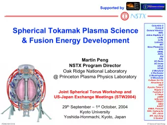
AFOSR Project Micro-Engineered Material Surfaces for Electric Propulsion and Pulsed Power PI: Nasr M. Ghoniem, UCLA Co-PI: Yevgeny Raitses, PPPL Kinetic Effects of Electron-Induced Secondary Electron Emission on Plasma -Wall Interactions
AFOSR Project Micro-Engineered Material Surfaces for Electric Propulsion and Pulsed Power PI: Nasr M. Ghoniem, UCLA Co-PI: Yevgeny Raitses, PPPL Kinetic Effects of Electron-Induced Secondary Electron Emission on Plasma -Wall Interactions Yevgeny Raitses and Igor D. Kaganovich Princeton Plasma Physics Laboratory Princeton, NJ 08543 2013 AFOSR Aerospace Materials for Extreme Environment (AMEE) Program 1 Review, February 11 - 15, 2013
Effects of Electron-Induced Secondary Electron Emission (SEE) on Plasma-Wall Interactions Yevgeny Raitses and Igor Kaganovich Status quo: Plasma with a strong SEE is relevant to plasma thrusters, high power MW devices, etc. Strong SEE can significantly alter plasma-wall interaction affecting thruster performance and lifetime. The observed SEE effects in thrusters requires fully kinetic modeling of plasma-wall interaction. New insight: Engineered materials with surface architecture can be used to control and suppress SEE. Project goal: Characterize effects of surface architecture on SEE and plasma-wall interaction Main accomplishments Surface architecture of engineered materials may Kinetic modeling predict new plasma regimes induce undesired electron field emission with strong SEE: unstable sheath, sheath collapse How it works: Nanocrystalline diamond coating exposed to plasma Plasma flow Three regimes for different effective SEE yield, l p Wall potential =0 oscillations <1 Velvet g Fibers >1 L 0 Sheath collapse wall heating No arcing No damage to diamond coating Wall Key publications in 2012 Phys. Rev. Lett. 108 , 255001; Phys. Rev. Lett. 108 , 235001 To avoid field emission g , l p < D , Debye length Phys. Plasmas 19 , 123513; Rev. Sci. Instr. 83 , 103502; 2 Phys. Plasmas 19 , 093511
Plasma-wall interaction in the presence of strong electron-induced secondary electron emission (SEE) • Any plasma with electron temperatures above 20 eV for dielectric walls, and above 50-100 eV for metal walls is subject to strong secondary electron emission (SEE) effects: Hall thrusters and Helicon thrusters Hollow cathodes for high power microwave electronics Multipactor breakdown and surface discharges Space plasmas and dusty plasmas Fusion plasmas Plasma processing discharges with RF or DC bias • Strong secondary electron emission from the floating walls can alter plasma -wall interaction and change plasma properties. • Strong SEE can significantly increase electron heat flux from plasma to the wall leading to: 1) wall heating and evaporation and 2) plasma cooling. 3
Hall Thruster (HT) – fuel-efficient plasma propulsion device for space applications Diameter ~ 1 -100 cm e Working gases: Xe, Kr e Pressure ~ 10 -4 torr Power ~ 0.1- 50 kW Boron nitride Thrust ~ 10 -3 - 1N ceramic channel Isp ~ 1000-3000 sec Efficiency up to 70% ü Hall thrusters can produce much higher thrust densities than ion thrusters 4
Plasma-wall interaction can deteriorate thruster performance and reduce thruster lifetime 1.35-kW SPT-100 New 1.35-kW SPT-100 5,700 Hrs 7 mm Courtesy: L. King F. Taccagona Boron nitride ceramic channel, 10 cm OD diameter 5
Electron emission from the wall can increase the plasma heat flux to the wall many times • Without SEE, sheath of space charge near the wall Hall thruster experiments show reflects most electrons back to the plasma, thus very different maximum electron effectively insulating wall from the plasma (Left Figure) temperatures with high and low SEE channel wall materials • SEE reduces the wall potential and allows large electron flux to the wall (Right Figure) w T e w 6T e i i e e see Y. Raitses et al., Phys. Plasmas Wall – Sheath - Plasma Wall - Sheath - Plasma 2005 6 Y. Raitses et al., IEEE TPS 2011
Electron-induced secondary electron emission (SEE) SEE Yield m SEE yield Energy Example of energy spectrum (for steel) Furman and Pivi, LBNL 52807, 2003 7
Secondary electron emission yield from dielectric materials Pz26 + Note: Pz26 - for Boron Nitride ceramic, if plasma (primary) electrons have Maxwellian electron energy distribution function (EEDF): Boron Nitride Teflon ( T e ) =1 at T e = 18.3 eV Dunaevsky et al., Phys. Plasmas, 2003 8
Upgraded setup for measurements of SEE yield from micro-engineered materials • Cryogenic system to maintain better vacuum (<10 -8 torr) during SEE measurements • Ion source to remove surface charges • The upgrade allows to minimize, outgassing, surface , contamination, etc. 9
Plasma properties can be changed by applying engineered materials to the surface Application of carbon velvet to channel walls improves considerably thruster Hall thruster performance by reducing the electron cross-field current and by increasing nearly twice the maximum electric field in the channel compared with the conventional BN ceramic walls. Plasma flow l p Velvet before plasma Velvet g Fibers L Channel wall Carbon Wall Protrusive velvet fibers > D To avoid field emission g, l p < Debye length Plasma burned out all • Velvet suppresses SEE and reduces current at high voltages (good) protrusive fibers • Sharp tips can enhance field emission leading to arcing (bad) • Need to engineer velvet morphology so that inter fiber gaps and protrusions are located well inside the sheath to avoid damage by arcing Need to take into account spatial and temporal variations of sheath Carbon 10 width due to plasma non-uniformity or instabilities velvet
Low Temperature Plasma Experiment (LTPX) was assembled to study kinetic effects of SEE on plasma properties Measured Electron Energy Distribution LTPX uses E B plasma discharge with easy Functions in LTPX access for probe and optical diagnostics Plasma operation with xenon gas • Hot electrons near the axis, R 2 cm, are due to electrons coming from cathode. • Electron energy near axis is 20-30 eV; that is sufficient to induce SEE from ceramic materials. • Electron energy can be additionally increased by application of higher bias voltage. 11
Experiments with micro- and nano-engineered materials immersed in LTPX plasma Micro-engineered materials are expected to minimize SEE, but may be a source of electron field emission due to surface irregularities. Electron field emission may weaken electrical and thermal insulating properties of the sheath similar to SEE effects. To evaluate possible effects of field and photoelectron emission, we immersed a 4” silicon wafer coated with ultrananocrystalline diamond (UNCD) in the plasma of LTPX setup. Ultrananocrystalline diamond has several nm’s grains with non-uniformities of up to 100’s nm and is often used as field emitter. Y. Raitses and A. V. Sumant, XXI International Material Research Congress , 2012 12
Characterization of electron emission from micro- and nano-engineered materials immersed in non-equilibrium plasma of LTPX Collector current vs. collector Main result: no difference was observed between probe bias voltage for UNCD and collector current measured with diamond and aluminum; aluminum collectors this suggests that the field emission from diamond is insignificant. According to the Fowler-Nordheim law, the field strength of E max E >10 3 kV/mm is required to produce an appreciable field-emission current. Here, is the field enhancement coefficient. In these experiments, the maximum electric field in the plasma-wafer sheath: E max ~ V b / D ~ 1 kV/mm. Here, V b is the bias voltage; D (Te/Ne) 0.5 3 10 -2 mm, is the Debye length. D is large compare to the grain size. Therefore, the field enhancement is negligible due to thick sheath 1. Electron field emission from micro-engineered materials facing the plasma should not be an issue as long as size of characteristic features of these materials is much smaller than the sheath size. 13
Surface coating can produce highly-localized plasma objects : Unipolar Arcs PPPL Magnetic Reconnection Experiment No arcs are observed on clean metal surface. Dielectric coating on metal wall promotes formation of unipolar arcs seen as blue spots of light. 14
Necessary conditions for unipolar arcing • Necessary conditions for unipolar arcing: Plasma E E - The sheath potential drop, V sh exceeds the + + breakdown/arc voltage. - Plasma can support sufficiently large arc current to form the spot, for example, by evaporating of wall Return current materials or producing thermionic or field emission. Schematics of current profiles in • Unipolar arcs also occur when walls are made from unipolar arc. micro-engineered material with complex surface - A. E. Robson and P. C. Thonemann, architecture. They were observed in PPPL Hall Proc. Phys. Soc. 1958 - A. V. Nedospasov and V. G. Petrov, thrusters experiments with carbon velvet walls. J. Nucl. Materials, 93, 1980 ü Arcing can induce permanent damage to walls ü Micro-engineered materials needs to be designed so that characteristic feature size is less than sheath. Plasma conditioning may remove features protruding above the sheath. ü Coatings needs to be removed. 15
Recommend
More recommend
Explore More Topics
Stay informed with curated content and fresh updates.
