In-Situ Correlative AFM/SEM/FIB Analysis of Nanostructures and - PowerPoint PPT Presentation
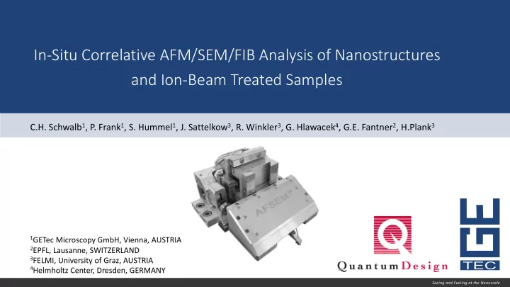
In-Situ Correlative AFM/SEM/FIB Analysis of Nanostructures and Ion-Beam Treated Samples C.H. Schwalb 1 , P. Frank 1 , S. Hummel 1 , J. Sattelkow 3 , R. Winkler 3 , G. Hlawacek 4 , G.E. Fantner 2 , H.Plank 3 1 GETec Microscopy GmbH, Vienna, AUSTRIA
In-Situ Correlative AFM/SEM/FIB Analysis of Nanostructures and Ion-Beam Treated Samples C.H. Schwalb 1 , P. Frank 1 , S. Hummel 1 , J. Sattelkow 3 , R. Winkler 3 , G. Hlawacek 4 , G.E. Fantner 2 , H.Plank 3 1 GETec Microscopy GmbH, Vienna, AUSTRIA 2 EPFL, Lausanne, SWITZERLAND 3 FELMI, University of Graz, AUSTRIA TEC 4 Helmholtz Center, Dresden, GERMANY Seeing and Feeling at the Nanoscale
Why do we believe in Correlative Analysis …? TEC Wha What you u typic pically ally see as as an an SEM us user… What you Wha u typic pically ally see as as an an AFM us user… Topography SEM AFSEM™ Conductivity Al Si Au EDX GETec Microscopy GmbH Seeing and Feeling at the Nanoscale 2
How can you find the interesting spot on this sample …? TEC GETec Microscopy GmbH Seeing and Feeling at the Nanoscale 3
Interactive Correlative SEM/AFM analysis of bone tissue TEC Direct ct acce ccess to 50 µm 3D t 3D topogr graphy in in the SEM 10 µm Sample courtesy: G. E. Fantner, EPFL, Lausanne GETec Microscopy GmbH Seeing and Feeling at the Nanoscale 4
Interactive Correlative SEM/AFM analysis of bone tissue TEC Direct access to 50 µm 3D topography in the SEM AF AFM hei eight cros oss sec ection on 10 µm Sample courtesy: G. E. Fantner, EPFL, Lausanne GETec Microscopy GmbH Seeing and Feeling at the Nanoscale 5
SEM, FIB, EDX, EBSD and AFM – A Perfect Fit … TEC 1. 1. Self-se sensi sing cantilevers 2. 2. Seamless Integration on Electrical cantilever readout Dedicated scanner design …BUT, it requires AFSEM™ goes to the AFSEM™ does NOT sample – interfere with „normal“ wherever it is… SEM operation 3. Easy and intuitive handling 3. 4. Matching imaging speed 4. AFSEM™ analysis in the SEM t SEM = t AFM a dedicated AFM How to quickly get to the AFSEM™ enables solution for SEM first correlative AFM/SEM interactive correlative image analysis (image < 1 min) GETec Microscopy GmbH Seeing and Feeling at the Nanoscale 6
Self-Sensing Cantilever Platform TEC Cantilever Platform 5 mm Thermal Standard Magnetic EBD Diamond Conductive GETec Microscopy GmbH Seeing and Feeling at the Nanoscale 7
Nanomechanics of free-standing nanowires TEC GETec Microscopy GmbH Seeing and Feeling at the Nanoscale 8
Nanomechanics of free-standing nanowires TEC SEM is crucial for positioning • of cantilever tip on nanowire AFSEM™ is crucial for • measurement of force- distance curves on free- standing nanowires structures True interactive experiment • GETec Microscopy GmbH Seeing and Feeling at the Nanoscale 9
3D subtractive tomography TEC GETec Microscopy GmbH Seeing and Feeling at the Nanoscale 10
FIB-assisted nanomechanical 3D reconstruction TEC Layer-by-layer nanomechanical analysis … 3D reconstructed nanomechanical properties GETec Microscopy GmbH Seeing and Feeling at the Nanoscale 11
AFSEM™ & He-Ions TEC Integration i In in O ORIO ION Na Nanofab Co Correlativ lative Interactiv active Analy nalysis is by merging the currently most advanced high-resolution triple-ion microscope with HIM HIM i image o of c cantilever the unique capabilities of the AFSEM™ GETec Microscopy GmbH Seeing and Feeling at the Nanoscale 12
In-Situ Correlative Analysis of Helium-treated samples TEC Implanted He bubbles in Si Silicon Nano-Pillars Cross-linked PMMA GETec Microscopy GmbH Seeing and Feeling at the Nanoscale 13
Working with combined strengths TEC GETec Microscopy GmbH Seeing and Feeling at the Nanoscale 14
MFM cantilever fabrication TEC 500 nm 200 nm CoFe tip deposition • Magnetic tip radius approx. 10 nm • Magnetic „Super“-tip allow for high-resolution magnetic imaging GETec Microscopy GmbH Seeing and Feeling at the Nanoscale 15
MFM image of FEBID CoFe disk/ring structure TEC SEM image of nanoscale in-situ 3D-printed magnetic CoFe structures 200 nm AFM topography MFM signal 3D topography with MFM signal overlay 100 nm 100 nm GETec Microscopy GmbH Seeing and Feeling at the Nanoscale 16
Correlative MFM of Nanomagnets TEC 500 nm GETec Microscopy GmbH Seeing and Feeling at the Nanoscale 17
Correlative Analysis – Application Examples in SEM or Dual-beam TEC Fracture Mechanics Electrical Characterization Measure simultaneously Localize fracture points with SEM and topography AND analyze in detail with the AFSEM™ spreading resistance Nano-Indentation Correlative AFM & EBSD Analyze surface changes after nano- Correlative SEM, EBSD and AFM analysis of indentation with sub-nm resolution ceramic materials GETec Microscopy GmbH Seeing and Feeling at the Nanoscale 18
AFSEM™ enhances YOUR SEM/Dual-beam TEC Cor Correlative Micros oscop opy Direct in-situ 3D-topography and roughness analysis without breaking vacuum To Topography and elemental analysis Measure shape and composition of your ? structures AF AFM & con onductivity or or magnetic prop oper erties es Measure the conductivity/magnetic properties of your structures with nanometer resolution AF AFM stiffn fnes ess analysis Measure the nano-mechanical properties of your structures Fo For more information vi visit t us … Your Application …? http://www.getec-afm.com/ TEC GETec Microscopy GmbH Seeing and Feeling at the Nanoscale 19
Recommend
More recommend
Explore More Topics
Stay informed with curated content and fresh updates.

