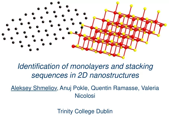

Identification of monolayers and stacking sequences in 2D nanostructures Aleksey Shmeliov, Anuj Pokle, Quentin Ramasse, Valeria Nicolosi Trinity College Dublin
Contents: 1. Introduction 2. 2D MoS 2 /WS 2 3. Black Phosphorous 4. Conclusions
2D-nanostructures In principle, any material with a layered structure can form 2D nanocrystals! Large range of materials: 1. Graphite, hBN, SnS 2 Potential Applications: 2. Transition Metal Chalcogenides 3. Transition Metal Oxides 1. Nanocomposites 2. Solar Cells All possible electronic properties: 3. Photocatalysts 1. Metals (NbSe 2 ) 4. Batteries 2. Semi-metals (graphene) 5. Supercapacitors 3. Semiconductors (WS 2 , MoS 2 ) 4. Insulators (MnO 2 ) 5. Superconductors (TaS 2 ) Charge-density waves (NbSe 2 ) 6. V. Nicolosi et al. “Liquid Exfoliation of Layered Materials,” Science, vol . 340, 2013
Production of 2D-nanostructures Micromechanical cleavage Chemical Vapour Deposition Liquid Phase Exfoliation: 1. via intercalated intermediate 2. via addition of surfactants 3. directly in solvent Stability of dispersions is achieved by matching surface energy of the 2D nanocrystal with the surface energy of the solvent! J.N. Coleman et al. “Two -Dimensional Nanosheets Produced by Liquid Exfoliation of Layered Materials,” Science , vol. 331, 2011, pp. 568-571
Mo/WS 2 structure
ADF STEM of MoS 2
ADF STEM of MoS 2
Non-bulk stacking
Black Phosphorous trilayer bilayer monolayer trilayer monolayer bilayer
Black Phosphorous R
Black Phosphorous
Conclusions Monolayers can be readily identified with ADF STEM 2D nanostructures do not necessarily have stacking of the bulk counterparts So far no-one published atomically resolved image of phosporene
ACKNOWLEDGEMENTS Peter Nellist Valeria Nicolosi Quentin Ramasse Peng Wang Anuj Pokle Mervyn Shannon Haibo E
Recommend
More recommend