Classical Control for Quantum Qubit decoherence Physical - PowerPoint PPT Presentation
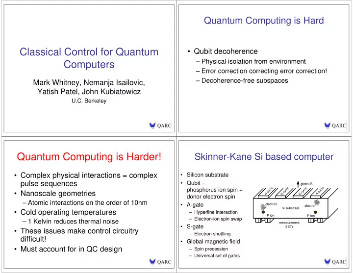
Quantum Computing is Hard Classical Control for Quantum Qubit decoherence Physical isolation from environment Computers Error correction correcting error correction! Decoherence-free subspaces Mark Whitney, Nemanja Isailovic,
Quantum Computing is Hard Classical Control for Quantum • Qubit decoherence – Physical isolation from environment Computers – Error correction correcting error correction! – Decoherence-free subspaces Mark Whitney, Nemanja Isailovic, Yatish Patel, John Kubiatowicz U.C. Berkeley Quantum Computing is Harder! Skinner-Kane Si based computer • Complex physical interactions = complex • Silicon substrate pulse sequences • Qubit = global B E E E E phosphorus ion spin + T T T T A A A A G G • Nanoscale geometries G G A - A - S - S - donor electron spin – Atomic interactions on the order of 10nm • A-gate electron electron Si substrate • Cold operating temperatures – Hyperfine interaction P ion P ion – Electron-ion spin swap – 1 Kelvin reduces thermal noise measurement • S-gate SETs • These issues make control circuitry – Electron shuttling difficult! • Global magnetic field • Must account for in QC design – Spin precession – Universal set of gates
Swap cell Quantum wires . . . . . . S A S A S S A S S A S S S . . . . . . A A A S A S S S S S S S S 4 2 1 0 0 2 1 4 1 4 3 5 5 3 4 1 S S A S S A • Ions are stationary e 1 - e 1 e 1 e 2 e 2 e 1 - - - - - e 2 e 2 e 1 e 1 - - - - e 2 e 1 e 1 e 2 - - - - e 2 e 1 e 1 e 2 e 2 - - - - - e 2 - – Qubits are moved by swapping • Alternating swap gives us “wires” e 2 - e 1 - Electron-ion spin swap – Some qubits move right, some left P ion 1 P ion 2 Electron-ion spin swap • Quantum wires seem more complicated than classical… • A lot of steps for two qubits! Swap Cell Control Pulse Sequence for 2-D Time Step 1 2 3 4 5 6 7 8 9 10 11 12 13 14 S 4 e 2 - e 2 - e 2 - e 2 - e 2 - e 2 - • 2-D layout (mentioned Electrons are too close A 2 e 2 - e 1 - e 2 - e 1 - Electrodes in Kane ’00) moves - - e 1 e 1 S 3 e 2 - S 1 S 2 S 3 e 2 - e 1 - e 1 - electrons in parallel e 1 - e 1 - e 1 - S 2 . . . . . . e 2 - e 2 e 1 - - A 1 A 2 – Simpler control - e 2 - e 2 A 1 e 1 - e 2 - e 2 - e 1 - – Better electron S 3 S 1 S 2 - - e 2 e 2 S 1 e 1 - e 1 - e 1 - e 1 - e 1 - separation e 1 - 24 A 1 24 24 A 1 ,A 2 • Control signals still Control A 2 signals S 1 S 1 complicated! S 2 S 2 – S-gate cascade S 3 S 3 Electron-ion spin swap – A-gate sequence S 4 • What a mess! Long pulse sequence…
Pulse Characteristics Qubit layout • voltage swing (V max ) adjusts d qubit • Clock rate . . . – Tuned for desired error rate – Electron-ion interaction period: • slew rate and clock period adjusts d Si e - 88.3ps -> 11.3GHz clock rate – Lowers electrode to back gate capacitance • Other technologies? (SOI) • Voltage swing • Pulse characteristics effect quantum datapath . . . . . . – Slower qubit manipulation d qubit e - – Lower voltage swing = lower voltage Gate Electrodes V max differential 0V d Si . . . . . . • Slew rate 0V – A-/S-gates must charge in clock period e - Single-electron transistors (SETs) Swap control circuit Control Input • S-/A-gate pulse Tunnel Junction - - e 1 e 1 sequences complex S 1 S 3 S 2 Island e 1 - - e 1 V DD . . . . . . • What would a circuit A 1 A 2 - e 2 - e 2 schematic look like? S 3 S 2 S 1 V DD e 2 - e 2 - C LOAD Y. Takahashi et. al. • CMOS does not work at 1K operating temperature 24 A 1 ,A 2 • SETs work well at low temperatures S 1 • Electrons move 1-by-1 through tunnel junction onto S 2 quantum dot and out other side S 3 • Low drive current (~5nA) and voltage swing (~40mV) – Affects our error and slew rates
Swap control circuit II Large! S 1 on S 1a S 3a S 2 on S 1b S 3b S 1 on S 3 on S 3 on S 1c S 3c A on S 4 on S 1d S 3d A a - - e 1 e 1 S 1 S 3 S 2 • Control circuit area, D D D D D D D S 2a S 4a S 2 on S 4 on - e 1 e 1 - S 2b S 4b . . . . . . S 1a S 2a S 3a S 3b S 4a S 1b ~10um 2 A 1 A 2 S-gate pulse cascade S 3c S 4b - e 2 - S 1c S 1d S 2b S 3d e 2 T – Aggressive process, S 3 S 1 D S 2 D D D D D D D - - e 2 e 2 30nm feature size – Minimal design Reset 24 7 A 1 ,A 2 4 3 2 1 0 • Swap cell area, 6 Reset S 1 5 8-bit counter 4 ~0.068um 2 A a 5-bit counter S 2 3 2 S 3 1 • Will not fit! Enable 0 A-gate pulse repeats 24 times Off-on A-gate pulse subsequence (2 off, 254 on) • Can this even be built with SETs? In SIMD we trust? Why on-chip? • Large control circuit/small swap cell ratio = SIMD • Like clock distribution network • Why not run many wires in from outside? • Clock skew at 11.3GHz? • Error correction • Error correction? complicates . . . . – Requires conditional . Swap . swapping S 3 A S 1 S 3 A S 1 S 2 S 2 Control 1000 qubits S 2 S 2 S 1 S 3 A S 1 S 3 A * 4 signals/qubit in swap S 2 S 2 S 2 S 2 S 1 A S 3 S 1 A S 3 * 336 swaps/lvl 1 ECC S 2 S 2 S 2 S 2 S 1 S 3 A S 1 S 3 = 1344000 wires! A S 2 S 2 1,000,000 wire bus! S 2 S 2 S 1 A S 3 . S 1 A S 3 • ECC could mean trouble . . . for SIMD in general . .
Conclusions • Pulse sequences for quantum gates are complex! • All quantum computing technologies require complex pulse sequences • Must keep control circuit in mind for large- scale integration
Recommend


More recommend
Explore More Topics
Stay informed with curated content and fresh updates.